SLOS882B January 2015 – December 2017 TPA3140D2
PRODUCTION DATA.
- 1 Features
- 2 Applications
- 3 Description
- 4 Revision History
- 5 Device Comparison Table
- 6 Pin Configuration and Functions
- 7 Specifications
- 8 Parameter Measurement Information
-
9 Detailed Description
- 9.1 Overview
- 9.2 Functional Block Diagram
- 9.3
Feature Description
- 9.3.1 Gain Setting via GAIN Pin
- 9.3.2 SD Operation
- 9.3.3 Gain Limit Control, LIMTHRES and LIMRATE
- 9.3.4 SPEAKERGUARD Automatic Gain Limit, AGL
- 9.3.5 Thermal Foldback, TFB
- 9.3.6 PLIMIT
- 9.3.7 LIMTHRES
- 9.3.8 Spread Spectrum and De-Phase Control
- 9.3.9 GVDD Supply
- 9.3.10 DC Detect
- 9.3.11 PBTL Select
- 9.3.12 Short-Circuit Protection and Automatic Recovery Feature
- 9.3.13 Thermal Protection
- 9.4 Device Functional Modes
-
10Application and Implementation
- 10.1 Application Information
- 10.2
Typical Applications
- 10.2.1 Design Requirements
- 10.2.2
Detailed Design Procedure
- 10.2.2.1 Ferrite Bead Filter Considerations
- 10.2.2.2 Efficiency: LC Filter Required with the Traditional Class-D Modulation Scheme
- 10.2.2.3 When to Use an Output Filter for EMI Suppression
- 10.2.2.4 Input Resistance
- 10.2.2.5 Input Capacitor, Ci
- 10.2.2.6 BSN and BSP Capacitors
- 10.2.2.7 Differential Inputs
- 10.2.2.8 Using Low-ESR Capacitors
- 10.2.3 Application Performance Curves
- 11Power Supply Recommendations
- 12Layout
- 13Device and Documentation Support
- 14Mechanical, Packaging, and Orderable Information
パッケージ・オプション
メカニカル・データ(パッケージ|ピン)
- PWP|28
サーマルパッド・メカニカル・データ
- PWP|28
発注情報
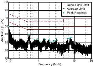
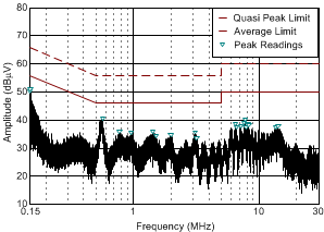
10.2.3.2 EN55022 Conducted Emissions Results
TV (40 inch) from the major TV manufacturer, TPA3140D2 EVM, PVCC = 12 V, 8-Ω speakers, Spread Spectrum enabled, PO = 1.25 W
| CISPR Class B 0.150-30MHz Idle Mode. SS0, Triangular, BD, 1.25 Watt |

| CISPR Class B 0.150-30MHz Idle Mode. SS0, Triangular, BD, 1.25 Watt |
Table 8. Conducted Emission - Line
| FREQUENCY MHz | QP LIMIT dBµV | AVE LIMIT dBµV | AVE READINGS dBµV | AVE MARGIN dB | QP READINGS dBµV | QP MARGIN dB |
|---|---|---|---|---|---|---|
| 0.156 | 65.83 | 55.83 | 33.774 | –22.056 | 45.956 | –19.873 |
| 0.552 | 56 | 46 | 28.872 | –17.128 | 39.164 | –16.836 |
| 0.806 | 56 | 46 | 21.341 | –24.659 | 29.585 | –26.415 |
| 0.95 | 56 | 46 | 22.678 | –23.322 | 31.471 | –24.529 |
| 1.485 | 56 | 46 | 22.622 | –23.378 | 31.082 | –24.918 |
| 1.976 | 56 | 46 | 20.952 | –25.048 | 29.849 | –26.151 |
Table 9. Conducted Emission - Neutral
| FREQUENCY MHz | QP LIMIT dBµV | AVE LIMIT dBµV | AVE READINGS dBµV | AVE MARGIN dB | QP READINGS dBµV | QP MARGIN dB |
|---|---|---|---|---|---|---|
| 0.158 | 65.785 | 55.785 | 34.022 | –21.763 | 45.398 | –20.387 |
| 0.554 | 56 | 46 | 29.574 | –16.426 | 40.485 | –15.515 |
| 0.735 | 56 | 46 | 22.652 | –23.348 | 32.52 | –23.48 |
| 0.918 | 56 | 46 | 22.699 | –23.301 | 31.849 | –24.151 |
| 1.402 | 56 | 46 | 23.264 | –22.736 | 32.173 | –23.827 |
| 7.806 | 60 | 50 | 28.006 | –21.994 | 35.214 | –24.786 |