SLOS907C April 2015 – December 2017 TPA3144D2
PRODUCTION DATA.
- 1 Features
- 2 Applications
- 3 Description
- 4 Revision History
- 5 Device Comparison Table
- 6 Pin Configuration and Functions
- 7 Specifications
- 8 Parameter Measurement Information
-
9 Detailed Description
- 9.1 Overview
- 9.2 Functional Block Diagram
- 9.3
Feature Description
- 9.3.1 Gain Setting via GAIN Pin
- 9.3.2 SD Operation
- 9.3.3 Gain Limit Control, LIMTHRES and LIMRATE
- 9.3.4 SPEAKERGUARD Automatic Gain Limit, AGL
- 9.3.5 Thermal Foldback, TFB
- 9.3.6 PLIMIT
- 9.3.7 LIMTHRES
- 9.3.8 Spread Spectrum and De-Phase Control
- 9.3.9 GVDD Supply
- 9.3.10 DC Detect
- 9.3.11 PBTL Select
- 9.3.12 Short-Circuit Protection and Automatic Recovery Feature
- 9.3.13 Thermal Protection
- 9.4 Device Functional Modes
-
10Application and Implementation
- 10.1 Application Information
- 10.2
Typical Applications
- 10.2.1 Design Requirements
- 10.2.2
Detailed Design Procedure
- 10.2.2.1 Ferrite Bead Filter Considerations
- 10.2.2.2 Efficiency: LC Filter Required with the Traditional Class-D Modulation Scheme
- 10.2.2.3 When to Use an Output Filter for EMI Suppression
- 10.2.2.4 Input Resistance
- 10.2.2.5 Input Capacitor, Ci
- 10.2.2.6 BSN and BSP Capacitors
- 10.2.2.7 Differential Inputs
- 10.2.2.8 Using Low-ESR Capacitors
- 10.2.3 Application Performance Curves
- 11Power Supply Recommendations
- 12Layout
- 13Device and Documentation Support
- 14Mechanical, Packaging, and Orderable Information
パッケージ・オプション
メカニカル・データ(パッケージ|ピン)
- PWP|28
サーマルパッド・メカニカル・データ
- PWP|28
発注情報
9.3.7 LIMTHRES
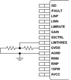
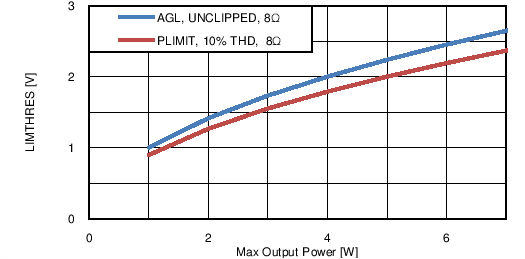
The AGL and PLIMIT voltage threshold is set by the applied LIMTHRES voltage. The LIMTHRES voltage is set by a voltage divider from GVDD to GND. The limiting is done by limiting the amplifier output voltage to a fixed maximum value. This limit can be thought of as a "virtual" voltage rail, which is lower than the PVCC supply. This virtual rail is 4 times the voltage at the LIMTHRES pin. This output voltage can be used to calculate the maximum output voltage (unclipped using AGL and clipped using PLIMIT) and power for a given LIMTHRES voltage and speaker impedance.

Where:
RS is the total series resistance including RDS(on), and any resistance in the output filter.
RL is the load resistance.
VP is the peak amplitude of the output possible within the supply rail.
VP = 4 × LIMTHRES voltage if VP < PVCC
POUT = Maximum unclipped output power. 10%THD using PLIMIT: 1.25 × PMAX (unclipped)
Increasing the LIMTHRES voltage from a given value increases the maximum output voltage swing until it equals PVCC. Adjusting LIMTHRES to a higher value will disable both the AGL and PLIMIT function and will offer highest available output power, however it is always advised to use the LIMTHRES function if PVCC is higher than the nominal value to prevent shutdown due to over current protection or to reduce frequency of thermal foldback events. To disable the AGL or PLIMIT function, the LIMTHRES pin is simply connected to GVDD.
 Figure 20. LIMHTRES Pin Voltage Programming by GVDD Resistor Divider
Table 3. LIMTHRES Typical Operation
| TEST CONDITIONS () | LIMTHRES VOLTAGE (V) | R to GND | R to GVDD | OUTPUT POWER (W), UNCLIPPED, AGL | OUTPUT POWER (W), 10% THD, PLIMIT |
| PVCC = 12 V, RL = 4 Ω | 1.6 | 22 kΩ | 68 kΩ | 4.75 | 6 |
| PVCC = 12 V, RL = 6 Ω | 1.9 | 33 kΩ | 82 kΩ | 4.75 | 6 |
| PVCC = 12 V, RL = 8 Ω | 2.2 | 39 kΩ | 82 kΩ | 4.75 | 6 |
space
 Figure 21. Max Output Power vs LIMTHRES, 8 Ω, PVCC = 12 V
 Figure 22. Max Output Power vs LIMTHRES, 6 Ω, PVCC = 12 V