JAJSD67A April 2016 – November 2016 TPA3244
PRODUCTION DATA.
- 1 特長
- 2 アプリケーション
- 3 概要
- 4 改訂履歴
- 5 Device Comparison Table
- 6 Pin Configuration and Functions
- 7 Specifications
- 8 Parameter Measurement Information
-
9 Detailed Description
- 9.1 Overview
- 9.2 Functional Block Diagrams
- 9.3 Feature Description
- 9.4
Device Functional Modes
- 9.4.1
Device Protection System
- 9.4.1.1 Overload and Short Circuit Current Protection
- 9.4.1.2 Signal Clipping and Pulse Injector
- 9.4.1.3 DC Speaker Protection
- 9.4.1.4 Pin-to-Pin Short Circuit Protection (PPSC)
- 9.4.1.5 Overtemperature Protection OTW and OTE
- 9.4.1.6 Undervoltage Protection (UVP) and Power-on Reset (POR)
- 9.4.1.7 Fault Handling
- 9.4.1.8 Device Reset
- 9.4.1
Device Protection System
-
10Application and Implementation
- 10.1 Application Information
- 10.2 Typical Applications
- 10.3 Typical Application, Differential (2N), PBTL (Outputs Paralleled after LC filter)
- 11Power Supply Recommendations
-
12Layout
- 12.1 Layout Guidelines
- 12.2
Layout Examples
- 12.2.1 BTL Application Printed Circuit Board Layout Example
- 12.2.2 SE Application Printed Circuit Board Layout Example
- 12.2.3 PBTL (Outputs Paralleled before LC filter) Application Printed Circuit Board Layout Example
- 12.2.4 PBTL (Outputs Paralleled after LC filter) Application Printed Circuit Board Layout Example
- 13デバイスおよびドキュメントのサポート
- 14メカニカル、パッケージ、および注文情報
パッケージ・オプション
デバイスごとのパッケージ図は、PDF版データシートをご参照ください。
メカニカル・データ(パッケージ|ピン)
- DDW|44
サーマルパッド・メカニカル・データ
発注情報
11 Power Supply Recommendations
11.1 Power Supplies
The TPA3244 device requires two external power supplies for proper operation. A high-voltage supply called PVDD is required to power the output stage of the speaker amplifier and its associated circuitry. Additionally, one mid-voltage power supply for GVDD_X and VDD is required to power the gate-drive and other internal digital and analog portions of the device. The allowable voltage range for both the PVDD and the GVDD_X/VDD supplies are listed in the Recommended Operating Conditions table. Ensure both the PVDD and the GVDD_X/VDD supplies can deliver more current than listed in the Electrical Characteristics table.
11.1.1 VDD Supply
The VDD supply required from the system is used to power several portions of the device. It provides power to internal regulators DVDD and AVDD that are used to power digital and analog sections of the device, respectively. Proper connection, routing, and decoupling techniques are highlighted in the TPA3244 Evaluation Module User's Guide (SLVUAT5) (as well as the Application Information section and Layout Examples section) and must be followed as closely as possible for proper operation and performance. Deviation from the guidance offered in the TPA3244 Evaluation Module User's Guide (SLVUAT5), which followed the same techniques as those shown in the Application Information section, may result in reduced performance, errant functionality, or even damage to the TPA3244 device. Some portions of the device also require a separate power supply which is a lower voltage than the VDD supply. To simplify the power supply requirements for the system, the TPA3244 device includes integrated low-dropout (LDO) linear regulators to create these supplies. These linear regulators are internally connected to the VDD supply and their outputs are presented on AVDD and DVDD pins, providing a connection point for an external bypass capacitors. It is important to note that the linear regulators integrated in the device have only been designed to support the current requirements of the internal circuitry, and should not be used to power any additional external circuitry. Additional loading on these pins could cause the voltage to sag and increase noise injection, which negatively affects the performance and operation of the device.
11.1.2 GVDD_X Supply
The GVDD_X supply required from the system is used to power the gate-drives for the output H-bridges. Proper connection, routing, and decoupling techniques are highlighted in the TPA3244 Evaluation Module User's Guide (SLVUAT5) (as well as the Application Information section and Layout Examples section) and must be followed as closely as possible for proper operation and performance. Deviation from the guidance offered in the TPA3244 device EVM User's Guide, which followed the same techniques as those shown in the Application Information section, may result in reduced performance, errant functionality, or even damage to the TPA3244 device.
11.1.3 PVDD Supply
The output stage of the amplifier drives the load using the PVDD supply. This is the power supply which provides the drive current to the load during playback. Proper connection, routing, and decoupling techniques are highlighted in the TPA3244 Evaluation Module User's Guide (SLVUAT5) (as well as the Application Information section and Layout Examples section) and must be followed as closely as possible for proper operation and performance. Due the high-voltage switching of the output stage, it is particularly important to properly decouple the output power stages in the manner described in the TPA3244 Evaluation Module User's Guide (SLVUAT5). The lack of proper decoupling, like that shown in the EVM User's Guide, can results in voltage spikes which can damage the device, or cause poor audio performance and device shutdown faults.
11.2 Powering Up
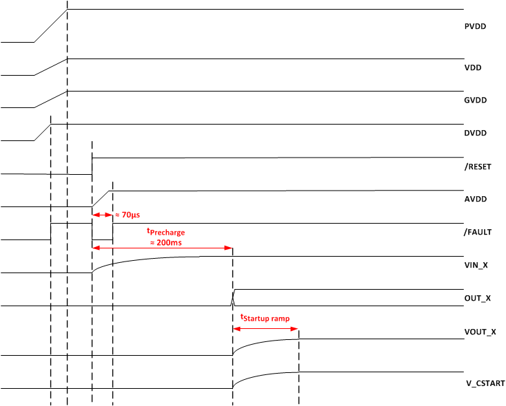
The TPA3244 device does not require a power-up sequence, but it is recommended to hold RESET low for at least 250 ms after PVDD supply voltage is turned ON. The outputs of the H-bridges remain in a high-impedance state until the gate-drive supply voltage (GVDD_X) and VDD voltages are above the undervoltage protection (UVP) voltage threshold (see the Electrical Characteristics table of this data sheet). This allows an internal circuit to charge the external bootstrap capacitors by enabling a weak pulldown of the half-bridge output as well as initiating a controlled ramp up sequence of the output voltage.
 Figure 27. Startup Timing
When RESET is released to turn on the TPA3244 device, FAULT signal will turn low and AVDD voltage regulator will be enabled. FAULT will stay low until AVDD reaches the undervoltage protection (UVP) voltage threshold (see the Electrical Characteristics table of this data sheet). After a precharge time to stabilize the DC voltage across the input AC coupling capacitors, before the ramp up sequence starts.
11.3 Powering Down
The TPA3244 device does not require a power-down sequence. The device remains fully operational as long as the gate-drive supply (GVDD_X) voltage and VDD voltage are above the undervoltage protection (UVP) voltage threshold. Although not specifically required, it is a good practice to hold RESET low during power down, thus preventing audible artifacts including pops or clicks by initiating a controlled ramp down sequence of the output voltage.
11.4 Thermal Design
11.4.1 Thermal Performance
The TPA3244 device thermal performance is dependent on the thermal design of the PCB. As a result, the maximum continuous output power attainable will be influenced by the PCB design. The continuous power rating is lower than the peak output power capability of the device. The peak power rating of the TPA3244 deviceis based on the burst capability of the device. The peak to average power ratio of the TPA3244 device is well suited to handle even demanding audio playback without thermal shutdown. Thermal performance with typical audio content (burst) versus sine wave content (continuous) should be considered when defining the thermal test requirements for the end product.
11.4.2 Thermal Performance with Continuous Output Power
It is recommended to operate the TPA3244 device below the OTW threshold, which in most systems will require the average output power to be below the maximum peak output power. The maximum continuous power, the TPA3244 device will deliver depends directly on the thermal design of the PCB and for the entire system (closed box with no air flow, or a fanned system etc.). Thermal performance is also impacted by PVDD voltage and switching frequency. The best configuration for a given application will often depend on the continuous output power requirements.
Table 15. Device and PCB Temperatures with 8-Ω Load, TA = 40°C
| TA = 40°C, TPA3244 EVM, No Airflow. Steady State Temperatures. | ||||||
|---|---|---|---|---|---|---|
| PVDD | Switching Frequency | Continuous Power [W] | Device Top Temperature | Maximum PCB Temperature | Comment | |
| 30V | 450kHz | 63W | 10% THD | 128ºC | 93ºC | OTW after 187 seconds. |
| 30V | 450kHz | 31.5W | 1/2 of 10% THD power | 111ºC | 83ºC | |
| 30V | 450kHz | 15.75W | 1/4 of 10% THD power | 89ºC | 71ºC | |
| 30V | 450kHz | 7.9W | 1/8 of 10% THD power | 76ºC | 63ºC | |
| 30V | 600kHz | 62W | 10% THD | 141ºC | 100ºC | OTW after 38 seconds. Not recommended. |
| 30V | 600kHz | 31W | 1/2 of 10% THD power | 130ºC | 94ºC | OTW after 205 seconds. |
| 30V | 600kHz | 15.5W | 1/4 of 10% THD power | 99ºC | 77ºC | |
| 30V | 600kHz | 7.75W | 1/8 of 10% THD power | 84ºC | 68ºC | |
Table 16. Device and PCB Temperatures with 4-Ω Load, TA = 40°C
| TA = 40°C, TPA3244 EVM, No Airflow. Steady State Temperatures. | ||||||
|---|---|---|---|---|---|---|
| PVDD | Switching Frequency | Continuous Power [W] | Device Top Temperature | Maximum PCB Temperature | Comment | |
| 30V | 450kHz | 114W | 10% THD | OTE(1) | OTW and OTE after less than 1 second. Not recommended. | |
| 30V | 450kHz | 57W | 1/2 of 10% THD power | OTE(1) | OTW after 3 seconds and OTE after 9 seconds. Not recommended. | |
| 30V | 450kHz | 28.5W | 1/4 of 10% THD power | OTE(1) | OTW after 44 seconds and OTE after 327 seconds. Not recommended. | |
| 30V | 450kHz | 14.25W | 1/8 of 10% THD power | 107ºC | 82ºC | |
| 30V | 600kHz | Not recommended | ||||
| 26V | 450kHz | 84W | 10% THD | OTE(1) | OTW after 3 seconds and OTE after 6 seconds. Not recommended. | |
| 26V | 450kHz | 42W | 1/2 of 10% THD power | OTE(1) | OTW after 15 seconds and OTE after 56 seconds. Not recommended. | |
| 26V | 450kHz | 21W | 1/4 of 10% THD power | 113ºC | 84ºC | |
| 26V | 450kHz | 10.5W | 1/8 of 10% THD power | 87ºC | 69ºC | |
| 26V | 600kHz | 83W | 10% THD | OTE(1) | OTW after 3 seconds and OTE after 6 seconds. Not recommended. | |
| 26V | 600kHz | 41.5W | 1/2 of 10% THD power | OTE(1) | OTW after 9 seconds and OTE after 30 seconds. Not recommended. | |
| 26V | 600kHz | 20.75W | 1/4 of 10% THD power | 129ºC | 93ºC | OTW after 301 seconds. |
| 30V | 600kHz | 10.50W | 1/8 of 10% THD power | 97ºC | 76ºC | |
11.4.3 Thermal Performance with Non-Continuous Output Power
As audio signals often have a peak to average ratio larger than one (average level below maximum peak output), the thermal performance for audio signals can be illustrated using burst signals with different burst ratios.
 Figure 28. Example of audio signal
A burst signal is characterized by the high-level to low-level ratio as well as the duration of the high level and low level, e.g. a burst 1:4 stimuli is a single period of high level followed by 4 cycles of low level.
 Figure 29. Example of 1:4 Burst Signal
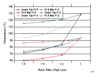
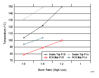
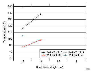
The following analysis of thermal performance for the TPA3244 device is made with the TPA3244 EVM surrounded by still air (no airflow) with a controlled air temperature of 40°C. For 30 V operation the system is not thermally limited with 8Ω load, but depending on the burst stimuli for operation at 30V some thermal limitations may occur, depending on switching frequency and average to maximum power ratio. Low to maximum power ratio of the burst stimuli is given in the plots as for example P1:8 which equals low level burst cycles of 1/8 power of the high level cycles. The level of the high power cycles is set equal to 10% THD level.

| PVDD = 30 V, fs = 450kHz | RL = 8Ω | TA = 40°C |

| PVDD = 26 V, fs = 450kHz | RL = 4Ω | TA = 40°C |

| PVDD = 30 V, fs = 600kHz | RL = 8Ω | TA = 40°C |

| PVDD = 26 V, fs = 600kHz | RL = 4Ω | TA = 40°C |