SLASE99A December 2015 – April 2016 TPA3250
PRODUCTION DATA.
- 1 Features
- 2 Applications
- 3 Description
- 4 Revision History
- 5 Device Comparison Table
- 6 Pin Configuration and Functions
-
7 Specifications
- 7.1 Absolute Maximum Ratings
- 7.2 ESD Ratings
- 7.3 Recommended Operating Conditions
- 7.4 Thermal Information
- 7.5 Electrical Characteristics
- 7.6 Audio Characteristics (BTL)
- 7.7 Audio Characteristics (SE)
- 7.8 Audio Characteristics (PBTL)
- 7.9 Typical Characteristics, BTL Configuration
- 7.10 Typical Characteristics, SE Configuration
- 7.11 Typical Characteristics, PBTL Configuration
- 8 Parameter Measurement Information
- 9 Detailed Description
- 10Application and Implementation
- 11Power Supply Recommendations
- 12Layout
- 13Device and Documentation Support
- 14Mechanical, Packaging, and Orderable Information
パッケージ・オプション
デバイスごとのパッケージ図は、PDF版データシートをご参照ください。
メカニカル・データ(パッケージ|ピン)
- DDW|44
サーマルパッド・メカニカル・データ
発注情報
1 Features
- Differential Analog Inputs
- Total Output Power at 10%THD+N
- 70-W Stereo Continuous into 8 Ω in BTL Configuration at 32 V
- 130-W Stereo Peak into 4 Ω in BTL Configuration at 32 V
- Total Output Power at 1%THD+N
- 60-W Stereo Continuous into 8 Ω in BTL Configuration at 32 V
- 105-W Stereo Peak into 4 Ω in BTL Configuration at 32 V
- Advanced Integrated Feedback Design with High-speed Gate Driver Error Correction
(PurePath™ Ultra-HD)- Signal Bandwidth up to 100 kHz for High Frequency Content From HD Sources
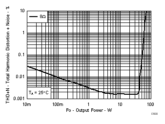
- Ultra Low 0.005% THD+N at 1 W into 4 Ω and <0.01% THD+N to Clipping
- 60 dB PSRR (BTL, No Input Signal)
- <60 µV (A-Weighted) Output Noise
- >110 dB (A Weighted) SNR
- Multiple Configurations Possible:
- Stereo, Mono, 2.1 and 4xSE
- Click and Pop Free Startup and Stop
- 92% Efficient Class-D Operation (8 Ω)
- Wide 12-V to 36-V Supply Voltage Operation
- Self-Protection Design (Including Undervoltage, Overtemperature, Clipping, and Short Circuit Protection) With Error Reporting
- EMI Compliant When Used With Recommended System Design
2 Applications
- High End Soundbar
- Mini Combo Systems
- Blu-ray Disk™ / DVD Receivers
- Active Speakers
3 Description
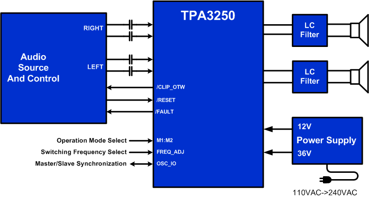
The TPA3250 device is a high performance class-D power amplifier that enables true premium sound quality with class-D efficiency. It features an advanced integrated feedback design and proprietary high-speed gate driver error correction (PurePath™ Ultra-HD). This technology allows ultra low distortion across the audio band and superior audio quality. With a 32V power supply the device can drive up to 2 x 130 W peak into 4-Ω load and 2 x 70 W continuous into 8-Ω load and features a 2 VRMS analog input interface that works seamlessly with high performance DACs such as TI's PCM5242. In addition to excellent audio performance, TPA3250 achieves both high power efficiency and very low power stage idle losses below 1 W. This is achieved through the use of 60 mΩ MOSFETs and an optimized gate driver scheme that achieves significantly lower idle losses than typical discrete implementations.
Device Information(1)
| PART NUMBER | PACKAGE | BODY SIZE (NOM) |
|---|---|---|
| TPA3250 | HTSSOP (44) | 6.10mm x 14.00mm |
- For all available packages, see the orderable addendum at the end of the datasheet.
Simplified Schematic

Total Harmonic Distortion
