SLOS490C July   2006  – November 2015

PRODUCTION DATA.  

  1. Features
  2. Applications
  3. Description
  4. Revision History
  5. Device Comparison Table
  6. Pin Configuration and Functions
  7. Specifications
    1. 7.1 Absolute Maximum Ratings
    2. 7.2 ESD Ratings
    3. 7.3 Recommended Operating Conditions
    4. 7.4 Thermal Information
    5. 7.5 Electrical Characteristics
    6. 7.6 Operating Characteristics
    7. 7.7 Dissipation Ratings
    8. 7.8 Typical Characteristics
  8. Parameter Measurement Information
  9. Detailed Description
    1. 9.1 Overview
    2. 9.2 Functional Block Diagram
    3. 9.3 Feature Description
      1. 9.3.1 Fully Differential Amplifiers
        1. 9.3.1.1 Advantages of Fully Differential Amplifiers
      2. 9.3.2 Fully Differential Amplifier Efficiency and Thermal Information
      3. 9.3.3 Differential Output Versus Single-Ended Output
    4. 9.4 Device Functional Modes
      1. 9.4.1 Summing Input Signals With The TPA6205A1
        1. 9.4.1.1 Summing Two Differential Input Signals
        2. 9.4.1.2 Summing a Differential Input Signal and a Single-Ended Input Signal
        3. 9.4.1.3 Summing Two Single-Ended Input Signals
      2. 9.4.2 Shutdown Mode
  10. 10Application and Implementation
    1. 10.1 Application Information
    2. 10.2 Typical Applications
      1. 10.2.1 TPA6205A1 With Differential Input
        1. 10.2.1.1 Design Requirements
        2. 10.2.1.2 Detailed Design Procedure
          1. 10.2.1.2.1 Selecting Components
            1. 10.2.1.2.1.1 Resistors (RF and RI)
            2. 10.2.1.2.1.2 Bypass Capacitor (CBYPASS) and Start-Up Time
            3. 10.2.1.2.1.3 Input Capacitor (CI)
            4. 10.2.1.2.1.4 Decoupling Capacitor (CS)
          2. 10.2.1.2.2 Using Low-ESR Capacitors
        3. 10.2.1.3 Application Curves
      2. 10.2.2 TPA6205A1 With Differential Input and Input Capacitors
        1. 10.2.2.1 Design Requirements
        2. 10.2.2.2 Detailed Design Procedure
        3. 10.2.2.3 Application Curves
      3. 10.2.3 TPA6205A1 With Single-Ended Input
        1. 10.2.3.1 Design Requirements
        2. 10.2.3.2 Detailed Design Procedure
        3. 10.2.3.3 Application Curves
  11. 11Power Supply Recommendations
    1. 11.1 Power Supply Decoupling Capacitors
  12. 12Layout
    1. 12.1 Layout Guidelines
    2. 12.2 Layout Example
  13. 13Device and Documentation Support
    1. 13.1 Community Resources
    2. 13.2 Trademarks
    3. 13.3 Electrostatic Discharge Caution
    4. 13.4 Glossary
  14. 14Mechanical, Packaging, and Orderable Information

パッケージ・オプション

メカニカル・データ(パッケージ|ピン)
サーマルパッド・メカニカル・データ
発注情報

6 Pin Configuration and Functions

ZQV Package
8-Pin BGA MICROSTAR JUNIOR
Top View
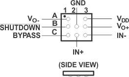
SLOS490TPA6205A1 po_01_slos490.gif
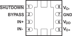
DRB Package
8-Pin SON
Top View
SLOS490TPA6205A1 po_02_slos490.gif
DGN Package
8-Pin MSOP-PowerPAD
Top View
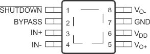
SLOS490TPA6205A1 po_03_slos490.gif

Pin Functions

PIN I/O DESCRIPTION
NAME BGA MICROSTAR JUNIOR SON,
MSOP-PowerPAD
BYPASS C1 2 I Mid-supply voltage. Adding a bypass capacitor improves PSRR.
GND B2 7 I High-current ground
IN– C3 4 I Negative differential input
IN+ C2 3 I Positive differential input
SHUTDOWN B1 1 I Shutdown terminal (active low logic)
VDD A3 6 I Supply voltage terminal
VO+ B3 5 O Positive BTL output
VO– A1 8 O Negative BTL output
Thermal Pad N/A Connect to ground. Thermal pad must be soldered down in all applications to properly secure device on the PCB.