JAJSD28A March 2017 – May 2017 TPD2S703-Q1
PRODUCTION DATA.
- 1 特長
- 2 アプリケーション
- 3 概要
- 4 改訂履歴
- 5 Pin Configuration and Functions
-
6 Specifications
- 6.1 Absolute Maximum Ratings
- 6.2 ESD Ratings—AEC Specification
- 6.3 ESD Ratings—IEC Specification
- 6.4 ESD Ratings—ISO Specification
- 6.5 Recommended Operating Conditions
- 6.6 Thermal Information
- 6.7 Electrical Characteristics
- 6.8 Power Supply and Supply Current Consumption Chracteristics
- 6.9 Timing Requirements
- 6.10 Typical Characteristics
- 7 Parameter Measurement Information
- 8 Detailed Description
- 9 Application and Implementation
- 10Power Supply Recommendations
- 11Layout
- 12デバイスおよびドキュメントのサポート
- 13メカニカル、パッケージ、および注文情報
パッケージ・オプション
メカニカル・データ(パッケージ|ピン)
サーマルパッド・メカニカル・データ
- DSK|10
発注情報
6 Specifications
6.1 Absolute Maximum Ratings
over operating free-air temperature range (unless otherwise noted) (1) (2)| MIN | MAX | UNIT | |||
|---|---|---|---|---|---|
| VPWR | 5-V DC supply voltage for internal circuitry | –0.3 | 7.7 |
V | |
| VREF | Pin to set OVP threshold | –0.3 | 6 | V | |
| VD+, VD– | Voltage range from connector-side USB data lines | –0.3 | 18 | V | |
| D+, D– | Voltage range for internal USB data lines | –0.3 | VREF + 0.3 | V | |
| VMODE | Voltage on MODE pin | –0.3 | 7.7 | V | |
| VFLT | Voltage on FLT pin | –0.3 | 7.7 | V | |
| VEN | Voltage on enable pin | –0.3 | 7.7 | V | |
| TA | Operating free air temperature(3) | –40 | 125 | °C | |
| TSTG | Storage temperature | –65 | 150 | °C | |
(1) Stresses beyond those listed under Absolute Maximum Ratings may cause permanent damage to the device. These are stress ratings only, which do not imply functional operation of the device at these or any other conditions beyond those indicated under Recommended Operating Conditions. Exposure to absolute-maximum-rated conditions for extended periods may affect device reliability.
(2) The algebraic convention, whereby the most negative value is a minimum and the most positive value is a maximum.
(3) Thermal limits and power dissipation limits must be observed.
6.2 ESD Ratings—AEC Specification
| VALUE | UNIT | ||||
|---|---|---|---|---|---|
| V(ESD) | Electrostatic discharge | Human-body model (HBM), per AEC Q100-002(1) | All pins | ±2000 | V |
| Charged-device model (CDM), per AEC Q100-011 | All pins besides corners | ±500 | |||
| Corner pins | ±750 | ||||
(1) AEC Q100-002 indicates that HBM stressing shall be in accordance with the ANSI/ESDA/JEDEC JS-001 specification.
6.3 ESD Ratings—IEC Specification
| VALUE | UNIT | ||||
|---|---|---|---|---|---|
| V(ESD) | Electrostatic discharge | IEC 61000-4-2 contact discharge | VD+, VD– pins(1) | ±8000 | V |
| IEC 61000-4-2 air-gap discharge | VD+, VD– pins(1) | ±15000 | |||
(1) See Figure 23 for details on system level ESD testing setup.
6.4 ESD Ratings—ISO Specification
| VALUE | UNIT | ||||
|---|---|---|---|---|---|
| VESD (1) | Electrostatic discharge | ISO 10605 (330 pF, 330 Ω) contact discharge (10 strikes) | VD+, VD– pins | ±8000 | V |
| ISO 10605 (330 pF, 330 Ω) air-gap discharge (10 strikes) | VD+, VD– pins | ±15000 | |||
| ISO 10605 (150 pF, 330 Ω) contact discharge (10 strikes) | VD+, VD– pins | ±8000 | |||
| ISO 10605 (150 pF, 330 Ω) air-gap discharge (10 strikes) | VD+, VD– pins | ±15000 | |||
| ISO 10605 (330 pF, 2 kΩ) contact discharge (10 stikes)(2) | VD+, VD– pins | ±8000 | |||
| ISO 10605 (330 pF, 2 kΩ) air-gap discharge (10 strikes) | VD+, VD– pins | ±15000 | |||
| ISO 10605 (150 pF, 2 kΩ) air-gap discharge (10 discharges) | VD+, VD– pins | ±25000 | |||
(1) See Figure 23 for details on system level ESD testing setup.
(2) VREF > 3 V.
6.5 Recommended Operating Conditions
over operating free-air temperature range (unless otherwise noted)| MIN | TYP | MAX | UNIT | |||
|---|---|---|---|---|---|---|
| VPWR | 5-V DC supply voltage for internal circuitry | 4.5 | 7 | V | ||
| VREF | Mode 0. Voltage range for VREF pin (for setting OVP threshold) | 3 | 3.6 | V | ||
| VREF | Mode 1. Voltage range for VREF pin (for setting OVP threshold) | 0.63 | 3.8 | V | ||
| VD+, VD– | Voltage range from connector-side USB data lines | 0 | 3.6 | V | ||
| D+, D– | Voltage range for internal USB data lines | 0 | 3.6 | V | ||
| VEN | Voltage range for enable | 0 | 7 | V | ||
| VFLT | Voltage range for FLT | 0 | 7 | V | ||
| IFLT | Current into open drain FLT pin FET | 0 | 3 | mA | ||
| CVPWR | VPWR capacitance(1) | VPWR pin | 1 | 10 | µF | |
| CVREF | VREF capacitance | VREF pin | 0.3 | 1 | 3 | µF |
| CMODE | Allowed parasitic capacitance on mode pin from PCB and mode 1 external resistors | 20 | pF | |||
| RMODE_0 | Resistance to GND to set to mode 0 | 2 | 2.6 | kΩ | ||
| RMODE_1 | Resistance to GND to set to mode 1 (calculate parallel combination of RTOP and RBOT) | 14 | 20 | kΩ | ||
(1) For recommended values for capacitors and resistors, the typical values assume a component placed on the board near the pin. Minimum and maximum values listed are inclusive of manufacturing tolerances, voltage derating, board capacitance, and temperature variation. The effective value presented should be within the minimum and maximums listed in the table.
6.6 Thermal Information
| THERMAL METRIC(1) | TPD2S703-Q1 | UNIT | ||
|---|---|---|---|---|
| DGS (VSSOP) | DSK (WSON) | |||
| 10 PINS | 10 PINS | |||
| θJA | Junction-to-ambient thermal resistance | 167.3 | 61.5 | °C/W |
| θJCtop | Junction-to-case (top) thermal resistance | 56.9 | 51.3 | °C/W |
| θJB | Junction-to-board thermal resistance | 87.6 | 34 | °C/W |
| ψJT | Junction-to-top characterization parameter | 7.7 | 1.3 | °C/W |
| ψJB | Junction-to-board characterization parameter | 86.2 | 34.3 | °C/W |
| θJCbot | Junction-to-case (bottom) thermal resistance | N/A | 7.7 | °C/W |
(1) For more information about traditional and new thermal metrics, see the Semiconductor and IC Package Thermal Metrics application report.
6.7 Electrical Characteristics
over operating free-air temperature range (unless otherwise noted)| PARAMETER | TEST CONDITIONS | MIN | TYP | MAX | UNIT | ||
|---|---|---|---|---|---|---|---|
| MODE 1 ADJUSTABLE VREF | |||||||
| VMODE_CMP | Mode 1 VREF feedback regulator voltage | VMODE | Standard mode 1 set-up. EN = 0 V. Once VREF = 3.3 V, measure voltage on mode pin | 0.47 | 0.5 | 0.53 | V |
| IMODE_LEAK | Mode pin mode 1 leakage current | IMODE | Standard mode 1. Remove RTOP and RBOT. Power up device and wait until start-up time has passed. Then force 0.53 V on the MODE pin and measure current into pin | 50 | 200 | nA | |
| VREF_ACCURACY | VREF accuracy | VREF | Informative, test parameters below; accuracy with RTOP and RBOT as ±1% resistors | –8% | 8% | ||
| VREF_3.3V | Mode 1 VREF set to 3.3 V | VREF | Standard mode 1 set-up. RTOP = 140 kΩ ± 1%, RBOT = 24.9 kΩ ± 1%. EN = 0. Measure value of VREF once it settles | 3.04 | 3.31 | 3.58 | V |
| VREF_0.66V | Mode 1 VREF set to 0.66 V | VREF | Standard mode 1 set-up. RTOP = 47.5 kΩ ± 1%, RBOT = 150 kΩ ± 1%.EN = 0. Measure value of VREF once it settles | 0.6 | 0.66 | 0.72 | V |
| VREF_3.8V | Mode 1 VREF set to 3.8 V | VREF | Standard mode 1 set-up. RTOP = 165 kΩ ± 1%, RBOT = 24.9 kΩ ± 1%. EN = 0. Measure value of VREF once it settles | 3.5 | 3.81 | 4.12 | V |
| EN, FLT PINS | |||||||
| VIH | High-level input voltage | EN | Mode 0. Connect VPWR = 5 V; VREF = 3.3 V; VD+ = 3.3 V; Set VIH(EN) = 0 V; Sweep VIH from 0 V to 1.4 V; Measure when D+ drops low (less than or equal to 5% of 3.3 V) from 3.3 V | 1.2 | V | ||
| Low-level input voltage | Mode 0. Connect VPWR = 5 V; VREF = 3.3 V; VD+ = 3.3 V. Set VIH(EN) = 3.3 V; Sweep VIH from 3.3 V to 0.5 V; Measure when D+ rise to 95% of 3.3 V from 0 V | 0.8 | |||||
| IIL | Input leakage current | EN | Mode 0. VPWR = 5 V; VREF = 3.3 V; VI (EN) = 3.3 V ; Measure current into EN pin | 1 | µA | ||
| VOL | Low-level output voltage | FLT | Mode 0. Drive the TPS2S703-Q1 in OVP to assert FLT pin. Source IOL = 1 mA into FLT pin and measure voltage on FLT pin when asserted | 0.4 | V | ||
| TSD_RISING | The rising over-temperature protection shutdown threshold | VPWR = 5 V, ENZ = 0 V, TA stepped up until FLTZ is asserted | 140 | 150 | 165 | ℃ | |
| TSD_FALLING | The falling over-temperature protection shutdown threshold | VPWR = 5 V, ENZ = 0 V, TA stepped down from TSD_RISING until FLTZ is cleared | 125 | 138 | 150 | ℃ | |
| TSD_HYST | The over-temperature protection shutdown threshold hysteresis | TSD_RISING – TSD_FALLING | 10 | 12 | 15 | ℃ | |
| OVP CIRCUIT—VD± | |||||||
| VOVP_RISING | Input overvoltage protection threshold, VREF > 3.6 V | VD± | Mode 1. Set VPWR = 5 V; EN = 0 V; RTOP = 165 kΩ, RBOT = 24.9 kΩ. Connect D± to 40-Ω load. Increase VD+ or VD– from 4.1 V to 4.9 V. Measure the value at which FLTZ is asserted | 4.3 | 4.5 | 4.7 | V |
| VOVP_RISING | Input overvoltage protection threshold | VD± | Mode 1. Set VPWR = 5 V; EN = 0 V; RTOP = 140 kΩ, RBOT = 24.9 kΩ. Increase VD+ or VD– from 3.6 V to 4.6 V. Measure the value at which FLTZ is asserted. Repeat for RTOP = 39 kΩ, RBOT = 150 kΩ. Increase VD+ or VD– from 0.6 V to 0.9 V. Measure the value at which FLTZ is asserted. See the resultant values meet the equation, and make sure to observe data switches turnoff. Also check for mode 0 when VREF = 3.3 V |
1.19 × VREF | 1.25 × VREF | 1.31 × VREF | V |
| VHYS_OVP | Hysteresis on OVP | VD± | Difference between rising and falling OVP thresholds on VD± | 25 | mV | ||
| VOVP_FALLING | Input overvoltage protection threshold | VD± | After collecting each rising OVP threshold, lower the VD± voltage until you see FLT deassert. This gives the falling OVP threshold. Use this value to calculate VHYS_OVP | VOVP_RISING – VHYS_OVP | V | ||
| IVD_LEAK_0 V | Leakage current on VD± during normal operation | VD± | Standard mode 0 or mode 1. Set VD± = 0 V. D± = floating. Measure current flowing into VD± | –0.1 | 0.1 | µA | |
| IVD_LEAK_3.6V | Leakage current on VD± during normal operation | VD± | Standard mode 0 or mode 1. Set VD± = 3.6 V. D± = floating. Measure current flowing into VD± | 2.5 | 4 | µA | |
| VOVP_3.3V | Input overvoltage threshold for VREF = 3.3 V | VD± | Standard mode 1. RTOP = 140 kΩ ± 1%, RBOT = 24.9 kΩ ± 1%. Connect D± to 40-Ω load. Measure the value at which FLTZ is asserted | 3.61 | 4.14 | 4.67 | V |
| VOVP_0.66V | Input overvoltage threshold for VREF = 0.66 V | VD± | Standard mode 1. RTOP = 47.5 kΩ ± 1%, RBOT = 150 kΩ ± 1%. Connect D± to 40-Ω load. Measure the value at which FLTZ is asserted | 0.72 | 0.83 | 0.94 | V |
| SHORT-TO-BATTERY | |||||||
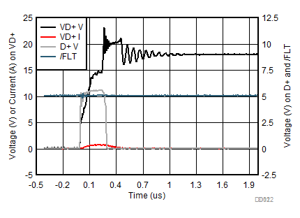
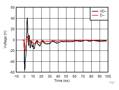
| VDATA_STB | Data line hotplug short-to-battery tolerance | V± | Charge battery-equivalent capacitor to test voltage then discharge to pin under test through a 1 meter, 18-ga wire. (See Figure 23 application information for more details) | 18 | V | ||
| VCLAMP_STB_DP/M_3V3 | Data line system side clamping voltage during STB | D± | Test both D+ and D– FETs. Test D+ and D– independently. Short VD+ and VD– to 18 V via hotplug to a battery-equivalent capacitor with a 1 meter, 18-ga wire. VREF = 3.3 V, VPWR = 5 V. Test in standard mode 0 and mode 1 | 5.5 | 6 | V | |
| VCLAMP_STB_DP/M_0V6 | Data line system side clamping voltage during STB | D± | Test both D+ and D– FETs. Short VD+ and VD– to 18 V via hotplug to a battery-equivalent capacitor with a 1 meter, 18-ga wire. VREF = 0.63 V, VPWR = 5 V. Test in standard mode 0 and mode 1 | 3.2 | 3.5 | V | |
| DATA LINE SWITCHES – VD+ to D+ or VD– to D– | |||||||
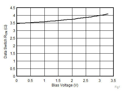
| RON | On resistance | Mode 0 or 1. Set VPWR = 5 V; VREF = 3.3 V; EN = 0 V; Measure resistance between D+ and VD+ or D– and VD–, voltage between 0 and 0.4 V | 4 | 6.5 | Ω | ||
| RON(Flat) | On resistance flatness | Mode 0 or 1. Set VPWR = 5 V; VREF = 3.3 V; EN = 0 V; Measure resistance between D+ and VD+ or D– and VD–, sweep voltage between 0 and 0.4 V. Take difference of resistance at 0.4-V and 0-V VD± bias | 1 | Ω | |||
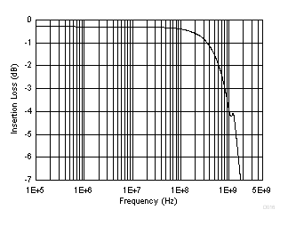
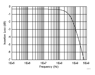
| BWON | On bandwidth (–3-dB) | Mode 0 or 1. Set VPWR = 5 V; VREF = 3.3 V; EN = 0 V; Measure S21 bandwidth from D+ to VD+ or D– to VD– with voltage swing = 400 mVpp, Vcm = 0.2 V | 960 | MHz | |||
6.8 Power Supply and Supply Current Consumption Chracteristics
over operating free-air temperature range (unless otherwise noted)| PARAMETER | TEST CONDITIONS | MIN | TYP | MAX | UNIT | |
|---|---|---|---|---|---|---|
| VUVLO_RISING_VPWR | VPWR rising UVLO threshold | Use standard mode 0 set-up. Set EN = 0 V, load D+ to 45 Ω, VD+ = 3.3 V. Set VPWR = 3.5 V, and step up VPWR until 90% of VD+ appears on D+ | 3.7 | 3.95 | 4.2 | V |
| VUVLO_HYST_VPWR | VPWR UVLO hysteresis | Use standard mode 0 set up. Set EN = 0 V, load D+ to 45 Ω, VD+ = 3.3 V. Set VPWR = 4.3 V, and step down VPWR until D+ falls to 10% of VD+. This gives VUVLO_FALLING_VPWR. VUVLO_RISING_VPWR – VUVLO_FALLING_VPWR = VUVLO_HYST_VPWR for this unit | 250 | 300 | 400 | mV |
| VUVLO_RISING_VREF | VREF rising UVLO threshold in mode 0 | Use standard mode 0 set up. Set EN = 0V, load D+ to 45 Ω, VD+ = 3.3 V. Set VREF = 2.5 V, and step up VREF until 90% of VD+ appears on D+ | 2.6 | 2.7 | 2.9 | V |
| VUVLO_HYST_VREF | VREF UVLO hysteresis | Use standard mode 0 set up. Set EN = 0 V, load D+ to 45 Ω, VD+ = 3.3 V. Set VREF = 3 V, and step down VREF until D+ falls to 10% of VD+. This gives VUVLO_FALLING_VREF. VUVLO_RISING_VREF –VUVLO_FALLING_VREF = VUVLO_HYST_VREF for this unit | 75 | 125 | 200 | mV |
| IVPWR_DISABLED_MODE0 | VPWR disabled current consumption | Use standard mode 0. EN = 5 V . Measure current into VPWR | 110 | µA | ||
| IVPWR_DISABLED_MODE1 | VPWR disabled current consumption | Use standard mode 1. EN = 5 V. Measure current into VPWR | 110 | µA | ||
| IVREF_DISABLED | VREF disabled current consumption mode 0 | Use standard mode 0. EN = 5 V. Measure current into VREF | 10 | µA | ||
| IVPWR_MODE0 | VPWR pperating current consumption | Use standard mode 0. EN = 0 V. Measure current into VPWR | 250 | µA | ||
| IVPWR_MODE1 | VPWR operating current consumption | Use standard mode 1. EN = 0 V. Measure current into VPWR | 350 | µA | ||
| IVREF | VREF operating current consumption mode 0 | Use standard mode 0. EN = 0 V. Measure current into VREF | 12 | 20 | µA | |
| ICHG_VREF | VREF fast charge current | Standard mode 1. 0.1 µF < CVREF < 3 µF. Set-up for charging to 3.3 V. Use a high voltage capacitor that does not derate capacitance up the 3.3 V. Measure slope to calculate the current when CVREF cap is being charged. Test to check this OPEN LOOP method | 22 | mA | ||
| ID_OFF_LEAK_STB | Mode 0. Measured flowing into D+ or D– supply, VPWR = 0 V, VD+ or VD– = 18 V, EN = 0 V, VREF = 0 V, D± = 0 V | –1 | 1 | µA | ||
| ID_ON_LEAK_STB | Mode 0. Measured flowing into D+ or D– supply, VPWR = 5 V, VD+ or VD– = 18 V, EN = 0 V, VREF = 3.3 V, D± = 0 V | –1 | 1 | µA | ||
| IVD_OFF_LEAK_STB | Mode 0. Measured flowing out of VD+ or VD– supply, VPWR = 0 V, VD+ or VD– = 18 V, EN = 0 V, VREF = 0 V, D± = 0 V | 120 | ||||
| IVD_ON_LEAK_STB | Mode 0. Measured flowing out of VD+ or VD– supply, VPWR = 5 V, VD+ or VD– = 18 V, EN = 0 V, VREF = 3.3 V, D± = 0 V | 120 | µA | |||
| IVPWR_TO_VREF_LEAK | Leakage from VPWR to VREF | Use standard mode 0. Set VREF = 0 V. Measured current flowing out of VREF pin | 1 | µA | ||
| IVREF_TO_VPWR_LEAK | Leakage from VREF to VPWR | Use standard mode 0. Set VPWR = 0 V. Measured as current flowing out of VPWR pin | 1 | µA | ||
6.9 Timing Requirements
over operating free-air temperature range (unless otherwise noted)| MIN | NOM | MAX | UNIT | |||
|---|---|---|---|---|---|---|
| ENABLE PIN AND VREF FAST CHARGE | ||||||
| TVREF_CHG | VREF fast charge time | Time between when 5 V is applied to VPWR, and VREF reaches VVREF_FAST_CHG. Needs to happen before or at same time tON_STARTUP completes | 0.5 | 1 | ms | |
| TON_STARTUP_MODE0 | Device turnon time from UVLO mode 0 | Mode 0. EN = 0 V, measured from VPWR and VREF = UVLO+ to data FET ON, VPWR comes to UVLO+ second. Place 3.3 V on VD±. Ramp VREF to 3.3 V, then VPWR to 5 V and measure the time it takes for D± to reach 90% of VD± | 0.5 | 1 | ms | |
| TON_STARTUP_MODE1 | Device turnon time from UVLO mode 1 | Informative. mode 1. EN = 0 V, measured from VPWR = UVLO+ to data FET ON | 0.5 + TCHG_CVREF | ms | ||
| TON_STARTUP_MODE1_3.3V | Device turnon time from UVLO mode 1 | Mode 1. EN = 0 V, measured from VPWR = UVLO+ to data FET ON, CVREF = 1 µF, VREF_FINAL = 3.3 V. Measure the time it takes for D± to reach 90% of VD± | 0.6 | 1 | ms | |
| TON_EN_MODE0 | Device turnon time mode 0 | Mode 0. VPWR = 5 V, VREF = 3.3 V, time from EN is asserted until data FET is ON. Place 3.3 V on VD±, measure the time it takes for D± to reach 90% of VD± | 150 | µs | ||
| TON_EN_MODE1 | Device turnon time mode 1 | Mode 1. VPWR = 5 V, VREF_INITIAL = 0 V, time from EN is asserted until data FET is ON. Place 3.3 V on VD±, measure the time it takes for D± to reach 90% of VD± | 150 + TCHG_VREF | µs | ||
| TON_EN_MODE1_3.3V | Device turnon time mode 1 for VREF = 3.3 V | Mode 1. VPWR = 5 V, VREF_INITIAL = 0 V, time from EN is asserted until data FET is ON. Place 3.3 V on VD±, measure the time it takes for D± to reach 90% of VD±. CVREF = 1 µF, VREF_FINAL = 3.3 V | 300 | µs | ||
| TOFF_EN | Device turnoff time | Mode 0 or 1. VPWR = 5 V, VREF = 3.3 V, time from EN is deasserted until data FET is off. Place 3.3 V on VD±, measure the time it takes for D± to fall to 10% of VD±, RD± = 45 Ω | 5 | µs | ||
| TCHG_CVREF | Time to charge CVREF | Informative. Mode 1. Time from VREF = 0 V to 80% × VREF_FINAL after EN transitions from high to low | (CVREF × 0.8 (VREF_FINAL)/(ICHG_VREF) | s | ||
| TCHG_CVREF_3.3V | Time to charge CVREF to 3.3 V | Mode 1. Time from VREF = 0 V to 90% × 3.3 V after EN transitions from high to low, CVREF = 1 µF | 132 | µs | ||
| TCHG_CVREF_0.66V | Time to charge CVREF to 0.66 V | Mode 1. Time from VREF = 0 V to 90% × 0.63 V after EN transitions from high to low, CVREF = 1 µF. RTOP = 47.5 kΩ ± 1%, RBOT = 150 kΩ ± 1% | 26 | µs | ||
| OVER VOLTAGE PROTECTION | ||||||
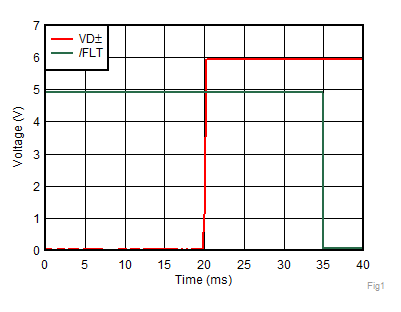
| tOVP_response_VBUS | OVP response time to VBUS | Mode 0 or 1. Measured from OVP condition to FET turn off . Short VD± to 5 V and measure the time it takes D± voltage to reach 0.1 × VD±_CLAMP_MAX from the time the 5-V hot-plug is applied. RLOAD_D± = 45 Ω.(1) (2) | 2 | µs | ||
| tOVP_response | OVP response time | Mode 0 or 1. Measured from OVP condition to FET turn off . Short VD± to 18 V and measure the time it takes D± voltage to reach 0.1 × VD±_CLAMP_MAX from the time the 18-V hot-plug is applied. RLOAD_D± = 45 Ω(1) (2) | 0.1 | 1 | µs | |
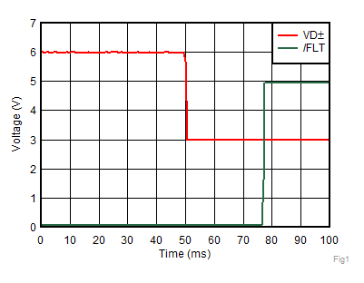
| tOVP_Recov _FLT | Recovery time FLT pin | Measured from OVP clear to FLT deassertion(1) | 32 | ms | ||
| tOVP_Recov _FET | Recovery time for data FET to turn back on | Measured from OVP clear until FET turns back on. Drop VD+ from 16 V to 3.3 V with VREF = 3.3 V, measure time it takes for D+ to reach 90% of 3.3 V | 32 | ms | ||
| tOVP_ASSERT | FLT assertion time | Measured from OVP on VD+ or VD– to FLT assertion | 12.6 | 18 | 23.4 | ms |
(1) Shown in Figure 1.
(2) Specified by design, not production tested.
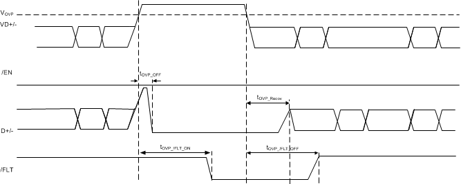
1. OVP Operation – VD+, VD–
Figure 1. TPD2S703-Q1 Timing Diagram
6.10 Typical Characteristics
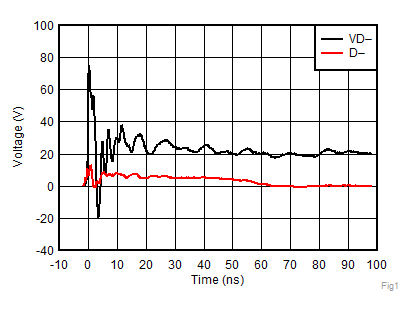
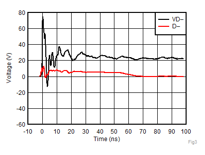
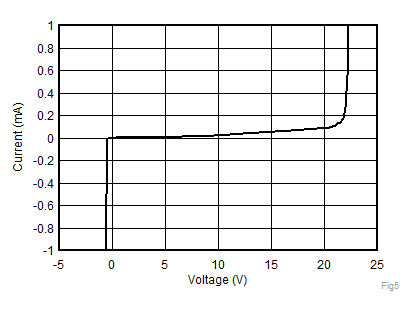
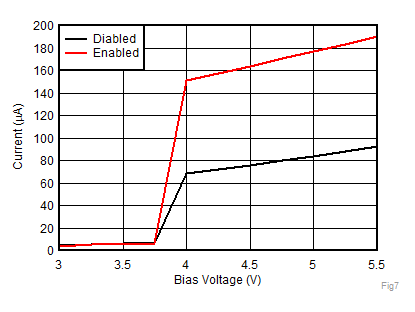
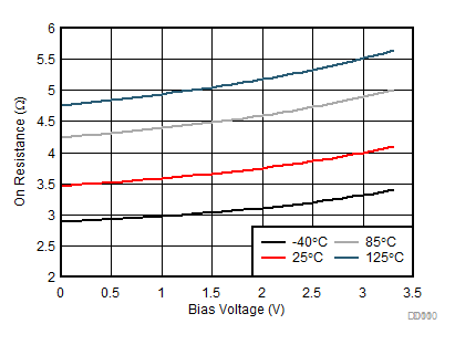
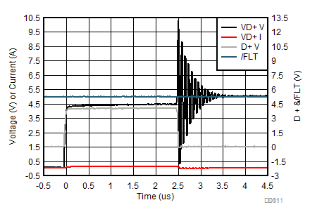
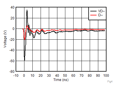
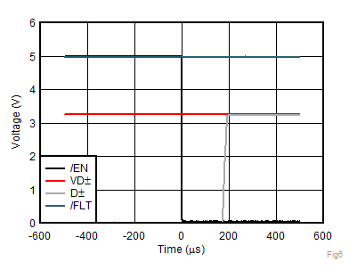
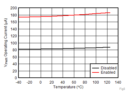
(VPWR = 5 V)
