SLVSCP4B October 2014 – August 2015 TPD3S014 , TPD3S044
PRODUCTION DATA.
- 1 Features
- 2 Applications
- 3 Description
- 4 Revision History
- 5 Device Comparison Table
- 6 Pin Configuration and Functions
- 7 Specifications
- 8 Detailed Description
- 9 Application and Implementation
- 10Power Supply Recommendations
- 11Layout
- 12Device and Documentation Support
- 13Mechanical, Packaging, and Orderable Information
11 Layout
11.1 Layout Guidelines
- The optimum placement is as close to the connector as possible.
- EMI during an ESD event can couple from the trace being struck to other nearby unprotected traces, resulting in early system failures.
- The PCB designer needs to minimize the possibility of EMI coupling by keeping any unprotected traces away from the protected traces which are between the TVS and the connector.
- Route the protected traces as straight as possible.
- Eliminate any sharp corners on the protected traces between the TVS and the connector by using rounded corners with the largest radii possible.
- Electric fields tend to build up on corners, increasing EMI coupling.
11.2 Layout Examples
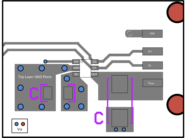
 Figure 36. USB2.0 Type A TPD3S0x4 Board Layout
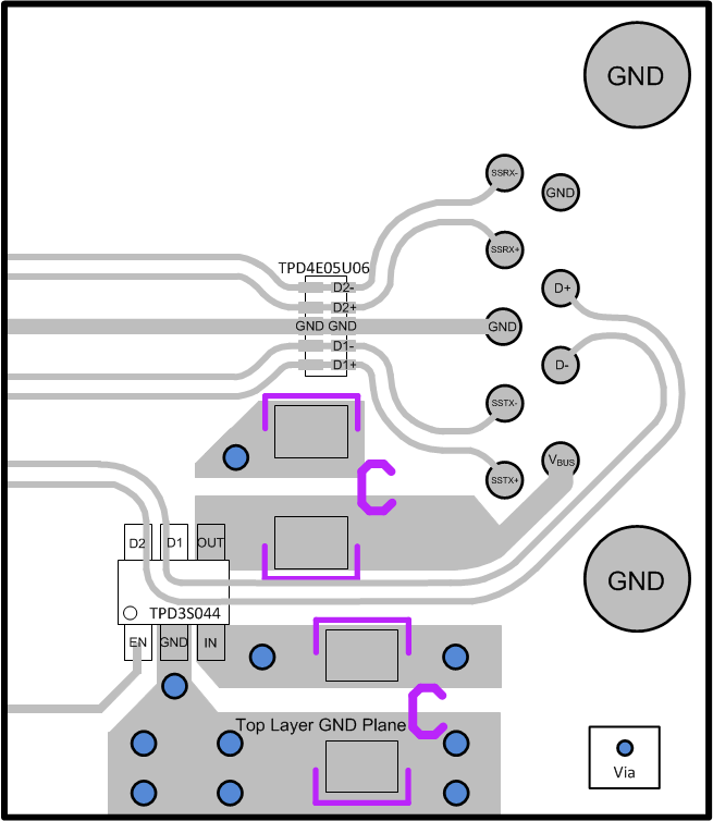
 Figure 37. USB3.0 Type A TPD3S044 Board Layout
11.3 Power Dissipation and Junction Temperature
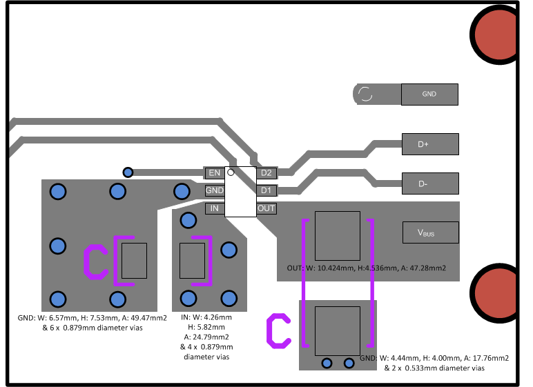
It is good design practice to estimate power dissipation and maximum expected junction temperature of the TPD3S0x4s. The system designer can control choices of the devices proximity to other power dissipating devices and printed circuit board (PCB) design based on these calculations. These have a direct influence on maximum junction temperature. Other factors, such as airflow and maximum ambient temperature, are often determined by system considerations. It is important to remember that these calculations do not include the effects of adjacent heat sources, and enhanced or restricted air flow. Addition of extra PCB copper area around these devices is recommended to reduce the thermal impedance and maintain the junction temperature as low as practical. In particular, connect the GND pin to a large ground plane for the best thermal dissipation. The following PCB layout example Figure 38 was used to determine the RθJA Custom thermal impedances noted in the Thermal Informationtable. It is based on the use of the JEDEC high-k circuit board construction with 4, 1 oz. copper weight layers (2 signal and 2 plane).
 Figure 38. PCB Layout Example
The following procedure requires iteration because power loss is due to the internal MOSFET I2 × RDS(ON), and RDS(ON) is a function of the junction temperature. As an initial estimate, use the RDS(ON) at 125°C from the Typical Characteristics, and the preferred package thermal resistance for the preferred board construction from the Thermal Information table.
where
- IOUT = Rated OUT pin current (A)
- RDS(ON) = Power switch on-resistance at an assumed TJ (Ω)
- TA = Maximum ambient temperature (°C)
- TJ = Maximum junction temperature (°C)
- RθJA = Thermal resistance (°C/W)
If the calculated TJ is substantially different from the original assumption, estimate a new value of RDS(ON) using the typical characteristic plot and recalculate.
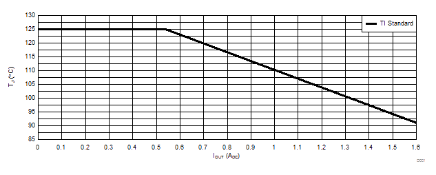
If the resulting TJ is not less than 125°C, try a PCB construction with a lower RθJA. Please find the junction temperature derating curve based on the TI standard reliability duration in Figure 39.
 Figure 39. Junction Temperature Derating Curve