JAJSJF0D March 2016 – August 2020 TPD3S716-Q1
PRODUCTION DATA
- 1 特長
- 2 アプリケーション
- 3 概要
- 4 Revision History
- 5 Pin Configuration and Functions
- 6 Specifications
- 7 Parameter Measurement Information
-
8 Detailed Description
- 8.1 Overview
- 8.2 Functional Block Diagram
- 8.3
Feature Description
- 8.3.1 AEC-Q100 Qualified
- 8.3.2 Short-to-Battery and Short-to-Ground Protection on VBUS_CON
- 8.3.3 Short-to-Battery and Short-to-VBUS Protection on VD+, VD–
- 8.3.4 ESD Protection on VBUS_CON, VD+, VD–
- 8.3.5 Low RON nFET VBUS Switch
- 8.3.6 High Speed Data Switches
- 8.3.7 Adjustable Hiccup Current Limit up to 2.4-A
- 8.3.8 Fast Over-Voltage Response Time
- 8.3.9 Independent VBUS and Data Enable Pins for Configuring both Host and Client/OTG Mode
- 8.3.10 Fault Output Signal
- 8.3.11 Thermal Shutdown Feature
- 8.3.12 16-Pin SSOP Package
- 8.3.13 Reverse Current Detection
- 8.4 Device Functional Modes
- 9 Application and Implementation
- 10Power Supply Recommendations
- 11Layout
- 12Device and Documentation Support
- 13Mechanical, Packaging, and Orderable Information
6.9 Typical Characteristics
 Figure 6-1 8-kV IEC Contact Waveform
 Figure 6-3 Data Line I-V Curve
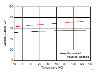 Figure 6-5 VD± Leakage Current at 18-V across Temperature
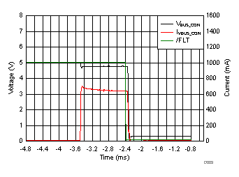 Figure 6-7 Overcurrent tBLANK Response Waveform
 Figure 6-9 VBUS Short-to-Ground Response Waveform
 Figure 6-11 Data Switch Short-to-5 V Response Waveform
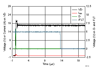 Figure 6-13 Data Switch Short-to-18 V Response Waveform (Long)
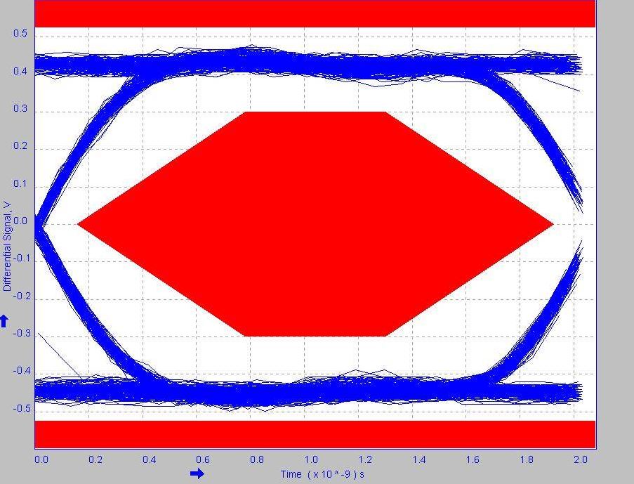 Figure 6-15 USB2.0 Eye Diagram (no TPD3S716-Q1)
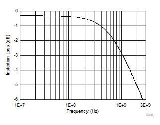 Figure 6-17 Data Switch Differential Bandwidth
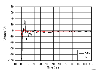 Figure 6-2 –8-kV IEC Contact Waveform
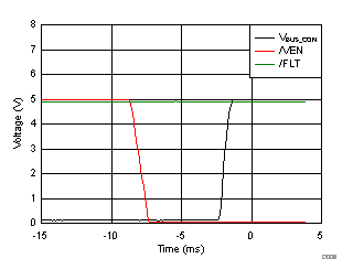 Figure 6-4 VBUS tON Time
 Figure 6-6 Data Switch RON vs Bias Voltage
 Figure 6-8 Overcurrent tBLANK_RETRY Response Waveform
 Figure 6-10 VBUS Short-to-18 V Response Waveform
 Figure 6-12 Data Switch Short-to-18 V Response Waveform
 Figure 6-14 Data Switch Crosstalk
 Figure 6-16 USB2.0 Eye Diagram (with TPD3S716-Q1)
 Figure 6-18 Data Switch Single-Ended Bandwidth