JAJSJJ7C December 2019 – February 2021 TPD4S311 , TPD4S311A
PRODUCTION DATA
- 1 特長
- 2 アプリケーション
- 3 概要
- 4 Revision History
- 5 Device Comparison Table
- 6 Pin Configuration and Functions
- 7 Specifications
-
8 Detailed Description
- 8.1 Overview
- 8.2 Functional Block Diagram
- 8.3
Feature Description
- 8.3.1 4-Channels of Short-to-VBUS Overvoltage Protection (CC1, CC2, SBU1, SBU2 Pins ): 24-VDC Tolerant
- 8.3.2 4-Channels of IEC 61000-4-2 ESD Protection (CC1, CC2, SBU1, SBU2 Pins)
- 8.3.3 CC1, CC2 Overvoltage Protection FETs 400-mA or 600-mA Capable for Passing VCONN Power
- 8.3.4 CC Dead Battery Resistors Integrated for Handling the Dead Battery Use Case in Mobile Devices
- 8.3.5 1.69-mm × 1.69-mm DSBGA Package
- 8.4 Device Functional Modes
- 9 Application and Implementation
- 10Power Supply Recommendations
- 11Layout
- 12Device and Documentation Support
- 13Mechanical, Packaging, and Orderable Information
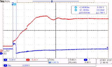
9.2.3 Application Curves
 Figure 9-3 TPD4S311 Turning On in Dead Battery Mode with RD
on CC1
 Figure 9-4 TPD4S311 Protecting the TPS65982 During a Short-to-VBUS Event