-
TPD7S019 7-Channel Integrated ESD Solution for VGA Port with Integrated Level-Shifter and Matching Impedance
- 1 Features
- 2 Applications
- 3 Description
- 4 Revision History
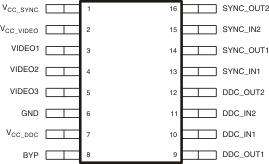
- 5 Pin Configuration and Functions
- 6 Specifications
- 7 Detailed Description
- 8 Application and Implementation
- 9 Power Supply Recommendations
- 10Layout
- 11Device and Documentation Support
- 12Mechanical, Packaging, and Orderable Information
- IMPORTANT NOTICE
パッケージ・オプション
メカニカル・データ(パッケージ|ピン)
サーマルパッド・メカニカル・データ
- RSV|16
発注情報
TPD7S019 7-Channel Integrated ESD Solution for VGA Port with Integrated Level-Shifter and Matching Impedance
1 Features
- 7-Channel ESD Protection Includes ESD Protection, Level-Shifting, Buffering and Sync Impedance Matching
- Exceeds IEC61000-4-2 (Level 4) ESD Protection to Requirements on the External Pins
- ±8-kV IEC 61000-4-2 Contact Discharge
- Very Low Loading Capacitance from ESD Protection Diodes on VIDEO Lines (2.5 pF)
- 5-V Drivers for HSYNC and VSYNC Lines
- Integrated Impedance Matching Resistors on Sync Lines
- Bidirectional Level-Shifting N-Channel FETs Provided for DDC_CLK and DDC_DATA Channels
- Flow-Through Single-In-Line Pin Mapping Ensures no Additional Board Layout Burden While Placing the ESD Protection Chip Near the Connector
2 Applications
- End Equipment:
- Desktop and Notebook PCs
- Set Top Boxes
- TVs
- Interfaces:
- VGA
- DVI-I
3 Description
The TPD7S019 device is an integrated electrostatic discharge (ESD) circuit protection solution for VGA and DVI-I connectors. It integrates transient voltage suppression (TVS) protection diodes for VIDEO, DDC and SYNC signals and meets the IEC61000-4-2 standard for ±8-kV contact ESD protection. The TVS diodes only add low capacitances to help signals run at high-speed. It also provides level-shifting for the DDC signals saving external level-shifters. Two noninverting drivers on HSYNC and VSYNC convert TTL input levels to CMOS output levels and each buffer has a series termination resistor connected to the SYNC_OUT pin, eliminating the external termination resistors. Three supply lines control the power rails of the VIDEO, DDC and SYNC channels to facilitate interfacing with low voltage video controller ICs in mixed supply-voltage environments. The TPD7S019 comes with two package options. The 16-pin RSV is compact and space-saving. The 16-pin DBQ package and pinout are optimized for easy board layout.
This ESD protection product is a good solution to protect the VGA and DVI-I ports for desktop and laptop PCs, set top boxes, TVs and monitors.
Device Information(1)
| PART NUMBER | PACKAGE | BODY SIZE (NOM) |
|---|---|---|
| TPD7S019 | SSOP (16) | 4.90 mm × 3.90 mm |
| UQFN (16) | 2.60 mm × 1.80 mm |
- For all available packages, see the orderable addendum at the end of the data sheet.
Application Schematic
.gif)
4 Revision History
Changes from D Revision (April 2016) to E Revision
Changes from C Revision (November 2015) to D Revision
- Updated the Functional Block DiagramGo
Changes from B Revision (December 2012) to C Revision
- Added Pin Configuration and Functions section, ESD Ratings table, Feature Description section, Device Functional Modes, Application and Implementation section, Power Supply Recommendations section, Layout section, Device and Documentation Support section, and Mechanical, Packaging, and Orderable Information section Go
Changes from * Revision (August 2010) to A Revision
- Removed PREVIEW status from the RSV package.Go
Changes from A Revision (March 2012) to B Revision
- Removed non released part descriptions from the datasheet.Go
5 Pin Configuration and Functions

Pin Functions
| PIN | TYPE | DESCRIPTION | ||
|---|---|---|---|---|
| NAME | DBQ | RSV | ||
| BYP | 8 | 6 | Power | Bypass pin. Using a 0.2-µF bypass capacitor increases the ESD robustness of the system |
| DDC_IN1 | 10 | 8 | I | DDC signal input. Connects to the VGA controller side of one of the sync lines |
| DDC_IN2 | 11 | 9 | ||
| DDC_OUT1 | 9 | 7 | O | DDC signal output. Connects to the video connector side of one of the sync lines |
| DDC_OUT2 | 12 | 10 | ||
| GND | 6 | 4 | — | Ground |
| SYNC_IN1 | 13 | 11 | I | Sync signal buffer input. Connects to the VGA controller side of one of the sync lines |
| SYNC_IN2 | 15 | 13 | ||
| SYNC_OUT1 | 14 | 12 | O | Sync signal buffer output. Connects to the video connector side of one of the sync lines |
| SYNC_OUT2 | 16 | 14 | ||
| VCC_DDC | 7 | 5 | Power | Isolated supply input for the DDC_1 and DDC_2 level-shifting N-FET gates |
| VCC_SYNC | 1 | 15 | Power | Isolated supply input for the SYNC_1 and SYNC_2 level-shifters and their associated ESD protection circuits |
| VCC_VIDEO | 2 | 16 | Power | Supply pin specifically for the VIDEO_1, VIDEO_2 and VIDEO_3 ESD protection circuits |
| VIDEO1 | 3 | 1 | ESD | High-speed ESD clamp input |
| VIDEO2 | 4 | 2 | ||
| VIDEO3 | 5 | 3 | ||
6 Specifications
6.1 Absolute Maximum Ratings
over operating free-air temperature range (unless otherwise noted)(1)| MIN | MAX | UNIT | |||||
|---|---|---|---|---|---|---|---|
| Supply voltage | VCC_VIDEO | –0.5 | 6 | V | |||
| VCC_DDC | –0.5 | 6 | |||||
| VCC_SYNC | –0.5 | 6 | |||||
| IO voltage | VIO(VIDEO) | VIDEOx pins | –0.5 | VCC_VIDEO | V | ||
| Input voltage | VI(SYNC) | SYNC pins | –0.5 | VCC_SYNC | V | ||
| VI(DDC) | DDC_INx pins | –0.5 | 6 | V | |||
| Output voltage | VO(DDC) | DDC_INx pins | –0.5 | 6 | V | ||
| Input clamp current | IIK | SYNC_INx, DDC_INx, VIDEOx | VI < 0 | –50 | mA | ||
| Output clamp current | IOK | SYNC_OUTx, DDC_OUTx | VO < 0 | –50 | mA | ||
| Continuous output current | IO | SYNC_OUTx | –24 | 24 | mA | ||
| DDC_INx to DDC_OUTx | –5 | 5 | mA | ||||
| Continuous current through supply pins | VCC_VIDEO, VCC_SYNC, VCC_DDC | –50 | 50 | mA | |||
| Storage temperature | Tstg | –55 | 125 | °C | |||
6.2 ESD Ratings
| VALUE | UNIT | ||||
|---|---|---|---|---|---|
| TPD7S019 in RSV Package | |||||
| V(ESD) | Electrostatic discharge | Human-body model (HBM), per ANSI/ESDA/JEDEC JS-001(1) | All pins except 1, 2, 3, 4, 7, 10, 12, and 14 | ±2000 | V |
| Pins 1, 2, 3, 7, 10, 12, and 14 | ±15000 | ||||
| Pin 4 | ±2000 | ||||
| Charged-device model (CDM), per JEDEC specification JESD22-C101(2) | ±1000 | ||||
| IEC 61000-4-2 contact discharge | Pins 1, 2, 3, 7, 10, 12, and 14 | ±8000 | |||
| TPD7S019 in DBQ Package | |||||
| V(ESD) | Electrostatic discharge | Human-body model (HBM), per ANSI/ESDA/JEDEC JS-001(1) | All pins except 3, 4, 5, 6, 9, 12, 14, and 16 | ±2000 | V |
| Pins 3, 4, 5, 9, 12, 14, and 16 | ±15000 | ||||
| Pin 6 | ±2000 | ||||
| Charged-device model (CDM), per JEDEC specification JESD22-C101(2) | ±1000 | ||||
| IEC 61000-4-2 contact discharge | Pins 3, 4, 5, 9, 12, 14, and 16 | ±8000 | |||
6.3 Recommended Operating Conditions
over operating free-air temperature range (unless otherwise noted)| MIN | MAX | UNIT | ||||
|---|---|---|---|---|---|---|
| Supply voltage | VCC_VIDEO | 0 | 5.5 | V | ||
| VCC_DDC | 0 | 5.5 | ||||
| VCC_SYNC | 0 | 5.5 | ||||
| IO voltage | VIO(VIDEO) | VIDEOx pins | 0 | VCC_VIDEO | V | |
| Input voltage | VI(SYNC) | SYNC pins | 0 | VCC_SYNC | V | |
| VI(DDC) | DDC_INx pins | 0 | 5.5 | V | ||
| Output voltage | VO(DDC) | DDC_INx Pins | 0 | 5.5 | V | |
| Operating temperature | TA | –40 | 85 | °C | ||
6.4 Thermal Information
| THERMAL METRIC(1) | TPD7S019 | UNIT | ||
|---|---|---|---|---|
| DBQ (SSOP) | RSV (UQFN) | |||
| 16 PINS | 16 PINS | |||
| RθJA | Junction-to-ambient thermal resistance | 115.8 | 124.5 | °C/W |
| RθJC(top) | Junction-to-case (top) thermal resistance | 67 | 52.7 | °C/W |
| RθJB | Junction-to-board thermal resistance | 58.3 | 53.8 | °C/W |
| ψJT | Junction-to-top characterization parameter | 19.9 | 1.4 | °C/W |
| ψJB | Junction-to-board characterization parameter | 57.9 | 53.8 | °C/W |
| RθJC(bot) | Junction-to-case (bottom) thermal resistance | N/A | N/A | °C/W |
6.5 Electrical Characteristics
over operating free-air temperature range (unless otherwise noted)| PARAMETER | TEST CONDITIONS | MIN | TYP | MAX | UNIT | |||
|---|---|---|---|---|---|---|---|---|
| ICC_VIDEO | VCC_VIDEO supply current | VCC_VIDEO = 5 V, VIDEO inputs at VCC_VIDEO or GND | 1 | 10 | µA | |||
| ICC_DDC | VCC_DDC supply current | VCC_DDC = 5 V | 1 | 10 | µA | |||
| ICC_SYNC | VCC_SYNC supply current | VCC_SYNC = 5 V | SYNC inputs at GND or VCC_SYNC, SYNC outputs unloaded |
1 | 50 | µA | ||
| SYNC inputs at 3 V; SYNC outputs unloaded |
2 | mA | ||||||
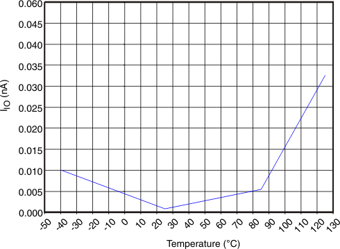
| IIO_VIDEO | VIDEO input and output pins | VIO_VIDEO = 3 V | 0.01 | 1 | µA | |||
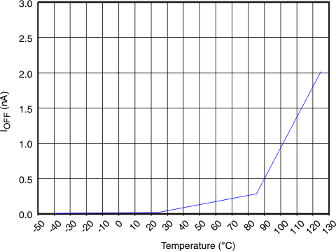
| IOFF | DDC pin power down leakage current | VCC_DDC ≤ 0.4 V, VDDC_OUT = 5 V | 0.01 | 1 | µA | |||
| VD | Diode forward voltage for lower clamp of VIDEO, DDC, SYNC output pins | ID = 8 mA, lower clamp diode | –0.6 | –0.8 | –0.95 | V | ||
| RDYN_VIDEO | Dynamic resistance (VIDEO pins) | I = 1 A | 1 | Ω | ||||
| VIH | High-level SYNC logic input voltage | VCC_SYNC = 5 V | 2 | V | ||||
| VIL | Low-level SYNC logic input voltage | VCC_SYNC = 5 V | 0.6 | V | ||||
| VOH | High-level SYNC logic output voltage | IOH = 0 mA, VCC_SYNC = 5 V | 4.85 | V | ||||
| VOH | High-level SYNC logic output voltage | IOH = –24 mA, VCC_SYNC = 5 V | 2 | V | ||||
| VOL | Low-level SYNC logic output voltage | IOL = 0 mA, VCC_SYNC = 5 V | 0.15 | V | ||||
| VOL | Low-level SYNC logic output voltage | IOL = 24 mA, VCC_SYNC = 5 V | 0.8 | V | ||||
| RT | SYNC driver output resistance | VCC_SYNC = 5 V, SYNC inputs at GND or 3 V | 15 | Ω | ||||
| CIO_VIDEO | IO capacitance of VIDEO pins | VIO = 2.5 V, test frequency is 1 MHz | 2.5 | 4 | pF | |||
| tPLH | SYNC driver L => H propagation delay | CL = 50 pF; VCC = 5 V, input tR and tF ≤ 5ns | 12 | ns | ||||
| tPHL | SYNC driver H => L propagation delay | CL = 50 pF; VCC = 5 V, input tR and tF ≤ 5ns | 12 | ns | ||||
| tR, tF | SYNC driver output rise & fall times | CL = 50 pF; VCC = 5 V, input tR and tF ≤ 5ns | 4 | ns | ||||
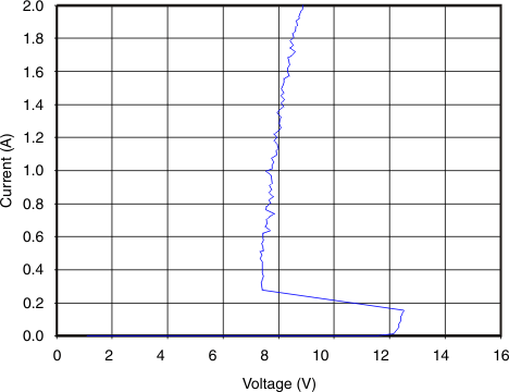
| VBR | VIDEO ESD diode break-down voltage | IIO = 1 mA | 9 | V | ||||
6.6 Typical Characteristics

 Figure 3. TPD7S019-xx IEC Clamping Waveforms Negative Contact

| VCC_DDC = 0 V |
 Figure 2. TPD7S019-xx IEC Clamping Waveforms Positive Contact

