SLVS816A July 2008 – December 2015 TPD8S009
PRODUCTION DATA.
- 1 Features
- 2 Applications
- 3 Description
- 4 Revision History
- 5 Pin Configuration and Functions
- 6 Specifications
- 7 Detailed Description
- 8 Application and Implementation
- 9 Power Supply Recommendations
- 10Layout
- 11Device and Documentation Support
- 12Mechanical, Packaging, and Orderable Information
パッケージ・オプション
メカニカル・データ(パッケージ|ピン)
- DSM|15
サーマルパッド・メカニカル・データ
- DSM|15
発注情報
8 Application and Implementation
NOTE
Information in the following applications sections is not part of the TI component specification, and TI does not warrant its accuracy or completeness. TI’s customers are responsible for determining suitability of components for their purposes. Customers should validate and test their design implementation to confirm system functionality.
8.1 Application Information
The TPD8S009 can provide system-level ESD protection to the high-speed differential lines of the HDMI or display ports. The flow-through package offers flexibility for board routing with traces up to 15-mm wide. Figure 5 shows the board-layout scheme for the four differential pair lines. The special pin configuration of the TPD8S009 matches the HDMI or DisplayPort pin assignments. It allows the differential signal pairs to couple together after they touch the ESD ports (pins 1–3, 4–6, 7–9, and 10–12) of the TPD8S009.
The TPD4E001 is recommended for ESD protection of slow-speed control lines.
8.2 Typical Application

8.2.1 Design Requirements
For this design example, one TPD8S009 devices, and one TPD4E001 are being used in an HDMI 1.4 application. This provides a complete port protection scheme.
Given the HDMI 1.4 application, the following parameters are shown in Table 1.
Table 1. Design Parameters
| DESIGN PARAMETER | VALUE |
|---|---|
| Signal range on high-speed TMDS pins | 0 V to 3.6 V |
| Operating Frequency | 1.7 GHz |
8.2.2 Detailed Design Procedure
To begin the design process, some parameters must be decided upon; the designer must know the following:
- Signal range on all the protected lines
- Operating frequency
8.2.2.1 Signal Range on High Speed TMDS Pins
TPD8S009 has 8 identical protection channels for signal lines. The symmetry of the device provides flexibility when selecting which of the 8 I/O channels protect which signal lines. The package is also designed to easily lay out on an HDMI connector, eliminating any tricky routing issues. Any I/O supports a signal range of 0 to 5.5 V. Therefore, this device supports the HDMI 1.4 signal swing.
8.2.2.2 Bandwidth on High-Speed TMDS Pins
Each pin of the TPD8S009 has a typical –3-dB bandwidth of 4GHz. Therefore, this device can handle HDMI 1.4 data rate of 3.4 Gbps with operating frequency of 1.7 GHz.
8.2.3 Application Curves
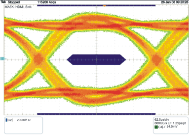
 Figure 6. Eye Diagram Without TPD8S009
 (2.5-Gbps Data Rate)
 Figure 7. Eye Diagram With TPD8S009
(2.5-Gbps Data Rate)