SLIS093D March 2000 – March 2015 TPIC6C596
PRODUCTION DATA.
- 1 Features
- 2 Applications
- 3 Description
- 4 Revision History
- 5 Pin Configuration and Functions
- 6 Specifications
- 7 Parameter Measurement Information
- 8 Detailed Description
- 9 Application and Implementation
- 10Power Supply Recommendations
- 11Layout
- 12Device and Documentation Support
- 13Mechanical, Packaging, and Orderable Information
パッケージ・オプション
デバイスごとのパッケージ図は、PDF版データシートをご参照ください。
メカニカル・データ(パッケージ|ピン)
- PW|16
- N|16
- D|16
サーマルパッド・メカニカル・データ
発注情報
8 Detailed Description
8.1 Overview
The TPIC6C596 device is a monolithic, medium-voltage, low-current 8-bit shift register designed to drive relatively moderate load power such as LEDs. The device contains a built-in voltage clamp on the outputs for inductive transient protection, so it can also drive relays, solenoids, and other low-current or medium-voltage loads.
8.2 Functional Block Diagram
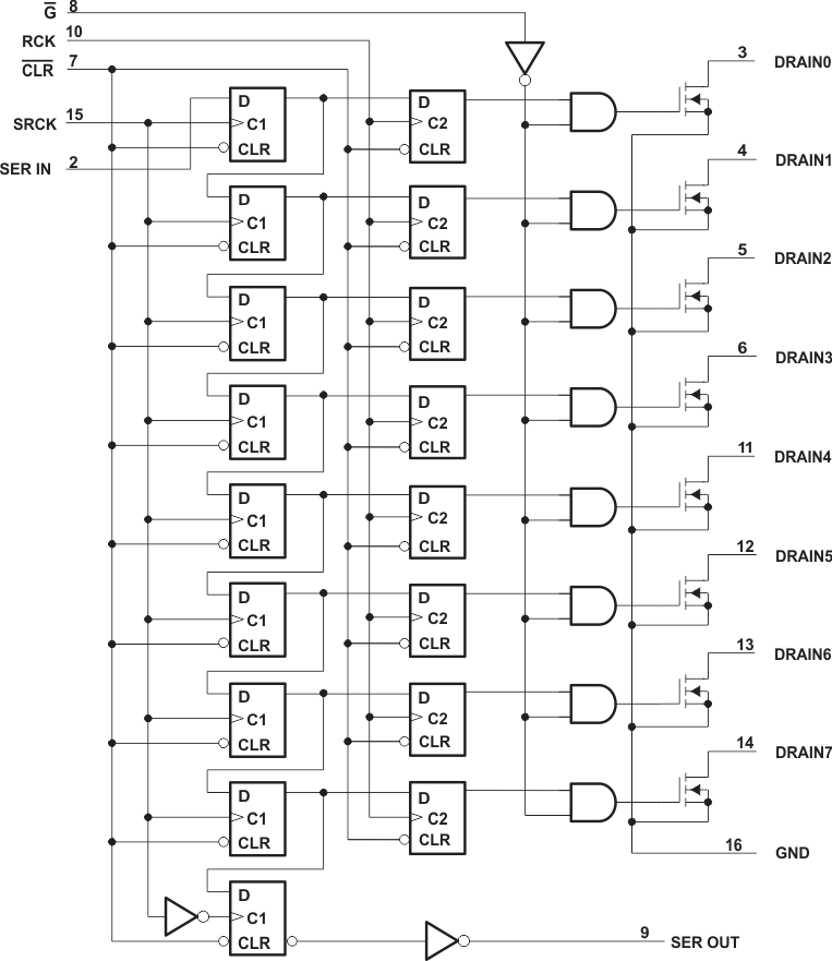
 Figure 12. Logic Diagram (Positive Logic)
8.3 Feature Description
8.3.1 Serial-In Interface
The TPIC6C596 device contains an 8-bit serial-in, parallel-out shift register that feeds an 8-bit D-type storage register. Data transfers through both the shift and storage registers on the rising edge of the shift register clock (SRCK) and the register clock (RCK), respectively. The storage register transfers data to the output buffer when shift register clear (CLR) is high.
8.3.2 Clear Register
A logical low on CLR clears all registers in the device. TI suggests clearing the device during power up or initialization.
8.3.3 Output Control
Holding the output enable (G) high holds all data in the output buffers low, and all drain outputs are off. Holding G low makes data from the storage register transparent to the output buffers. When data in the output buffers is low, the DMOS transistor outputs are off. When data is high, the DMOS transistor outputs are capable of sink-current. This pin can also be used for global PWM dimming.
8.4 Device Functional Modes
8.4.1 Operation With V(VIN) < 4.5 V (Minimum V(VIN))
This device works normally during 4.5 V ≤ V(VIN) ≤ 5.5 V, when operation voltage is lower than 4.5 V. The behavior of device can't be ensured, including communication interface and current capability.
8.4.2 Operating With 5.5 V < V(VIN) < 6 V
This device works normally during this voltage range, but reliability issues may occurs while the device works for a long time in this voltage range.