SLIS093D March 2000 – March 2015 TPIC6C596
PRODUCTION DATA.
- 1 Features
- 2 Applications
- 3 Description
- 4 Revision History
- 5 Pin Configuration and Functions
- 6 Specifications
- 7 Parameter Measurement Information
- 8 Detailed Description
- 9 Application and Implementation
- 10Power Supply Recommendations
- 11Layout
- 12Device and Documentation Support
- 13Mechanical, Packaging, and Orderable Information
パッケージ・オプション
デバイスごとのパッケージ図は、PDF版データシートをご参照ください。
メカニカル・データ(パッケージ|ピン)
- PW|16
- N|16
- D|16
サーマルパッド・メカニカル・データ
発注情報
11 Layout
11.1 Layout Guidelines
There is no special layout requirement for the digital signal pin; the only requirement is placing the ceramic bypass capacitors near the corresponding pin. Because the TPIC6C596 device does not have a thermal shutdown protection function, to prevent thermal damage, TJ must be less than 150°C. If the total sink current is high, the power dissipation might be large. The devices are currently not available in the thermal pad package, so good PCB design can optimize heat transfer, which is absolutely essential for the long-term reliability of the device.
Maximize the copper coverage on the PCB to increase the thermal conductivity of the board, because the major heat-flow path from the package to the ambient is through the copper on the PCB. Maximum copper is extremely important when the design does not include heat sinks attached to the PCB on the other side of the package.
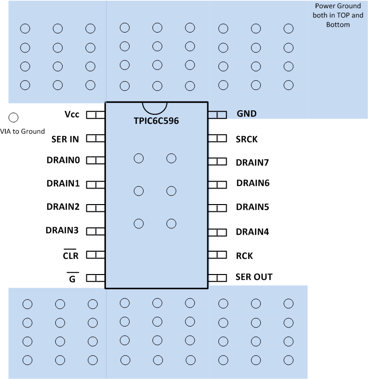
- Add as many thermal vias as possible directly under the package ground pad to optimize the thermal conductivity of the board.
- All thermal vias should be either plated shut or plugged and capped on both sides of the board to prevent solder voids. To ensure reliability and performance, the solder coverage should be at least 85%.
11.2 Layout Example
 Figure 16. Recommended Layout Example
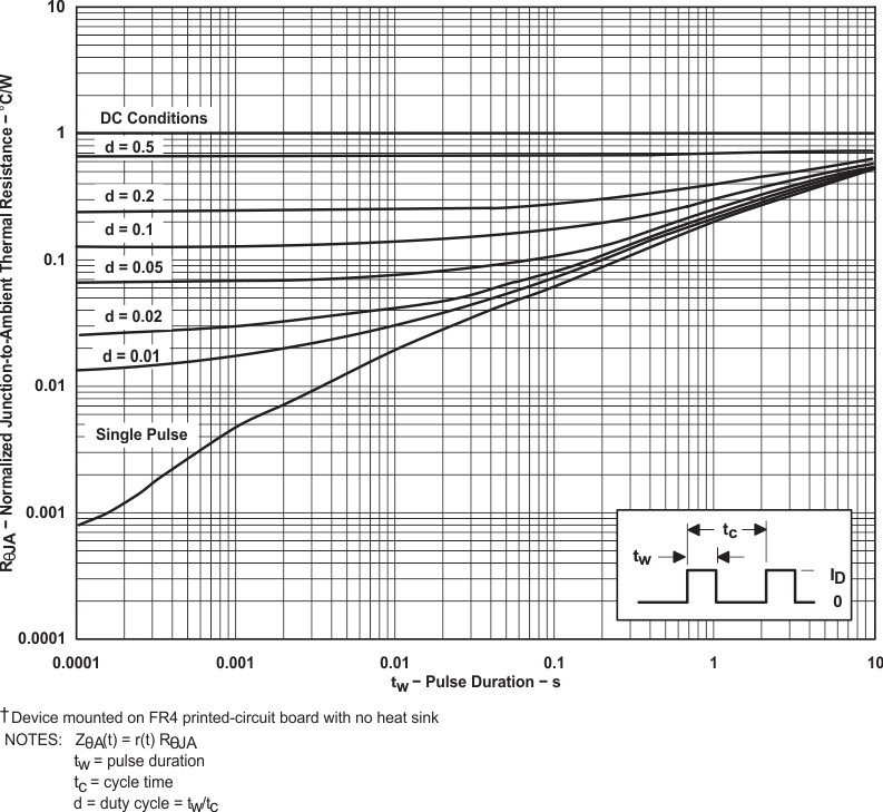
11.3 Thermal Considerations
 Figure 17. D Package†, Normalized Junction-to-Ambient Thermal Resistance vs Pulse Duration