SLIS110C April 2003 – March 2015 TPIC8101
PRODUCTION DATA.
- 1 Features
- 2 Applications
- 3 Description
- 4 Revision History
- 5 Description (continued)
- 6 Pin Configuration and Functions
- 7 Specifications
-
8 Detailed Description
- 8.1 Overview
- 8.2 Functional Block Diagram
- 8.3
Feature Description
- 8.3.1
Functional Terminal Description
- 8.3.1.1 Supply Voltage (VDD)
- 8.3.1.2 Ground (GND)
- 8.3.1.3 Reference Supply (Vref)
- 8.3.1.4 Buffered Integrator Output (OUT)
- 8.3.1.5 Integration/Hold Mode Selection (INT/HOLD)
- 8.3.1.6 Chip Select for SPI (CS)
- 8.3.1.7 Oscillator Input (XIN)
- 8.3.1.8 Oscillator Output (XOUT)
- 8.3.1.9 Data Output (SDO)
- 8.3.1.10 Data Input (SDI)
- 8.3.1.11 Serial Clock (SCLK)
- 8.3.1.12 Test (TEST)
- 8.3.1.13 Feedback Output for Amplifiers (CH1FB and CH2FB)
- 8.3.1.14 Input Amplifiers (CH1P, CH1N, CH2P, and CH2N)
- 8.3.2 Timing Information
- 8.3.1
Functional Terminal Description
- 8.4 Device Functional Modes
- 8.5 Programming
- 9 Application and Implementation
- 10Power Supply Recommendations
- 11Layout
- 12Device and Documentation Support
- 13Mechanical, Packaging, and Orderable Information
7 Specifications
7.1 Absolute Maximum Ratings
over operating free-air temperature range (unless otherwise noted) (1)| MIN | MAX | UNIT | ||
|---|---|---|---|---|
| VDD | Regulated input voltage (2)(3) | −0.3 | 7 | V |
| VO | Output voltage(2)(3) | −0.3 | 7 | V |
| VIN | Input voltage(2)(3) | −0.3 | 7 | V |
| IIN | DC input current on terminals CH1P, CH1N, CH2P, and CH2N(2)(3) | 2 | mA | |
| VDCIN | DC input voltage on terminals CH1P, CH1N, CH2P and CH2N(2)(3) | 14 | V | |
| RθJA | Junction-to-ambient thermal impedance | 120 | °C/W | |
| PD | Continuous power dissipation | 200 | mW | |
| TA | Operating ambient temperature | –40 | 125 | °C |
| Tstg | Storage temperature | –65 | 150 | °C |
(1) Stresses beyond those listed under Absolute Maximum Ratings may cause permanent damage to the device. These are stress ratings only, which do not imply functional operation of the device at these or any other conditions beyond those indicated under Recommended Operating Conditions. Exposure to absolute-maximum-rated conditions for extended periods may affect device reliability.
(2) All voltage values are with respect to GND.
(3) Absolute negative voltage on these terminals is not to go < –0.5 V.
7.2 ESD Ratings
| VALUE | UNIT | |||
|---|---|---|---|---|
| V(ESD) | Electrostatic discharge | Human-body model (HBM)(1) | 4000 | V |
| Charged-device model (CDM) | 1500 | |||
(1) The human body model is a 100-pF capacitor discharged through a 1.5-kΩ resistor into each terminal.
7.3 Recommended Operating Conditions
over operating free-air temperature range (unless otherwise noted)| MIN | MAX | UNIT | ||
|---|---|---|---|---|
| VDD | Regulated input voltage | −0.3 | 5.5 | V |
| VO | Output voltage | −0.3 | 5.5 | V |
| VIN | Input voltage | 0.05 | VDD − 0.05 | V |
| IIN | DC input current on terminals CH1P, CH1N, CH2P, and CH2N | –1 | 1 | µA |
| VDCIN | DC input voltage on terminals CH1P, CH1N, CH2P, and CH2N | Vref, (VDD / 2) | V | |
| PD | Continuous power dissipation | 100 | mW |
7.4 Thermal Information
| THERMAL METRIC(1) | TPIC8101 | UNIT | |
|---|---|---|---|
| DW [SOIC] | |||
| 20 PINS | |||
| RθJA | Junction-to-ambient thermal resistance | 66.2 | °C/W |
| RθJC(top) | Junction-to-case (top) thermal resistance | 29.6 | |
| RθJB | Junction-to-board thermal resistance | 34.4 | |
| ψJT | Junction-to-top characterization parameter | 7.1 | |
| ψJB | Junction-to-board characterization parameter | 33.8 | |
(1) For more information about traditional and new thermal metrics, see the IC Package Thermal Metrics application report, SPRA953.
7.5 Electrical Characteristics
VDD = 5 V ±5%, input frequency before prescaler = 4 to 20 MHz (±0.5%), TA = −40°C to 125°C (unless otherwise specified)| PARAMETER | TEST CONDITIONS | MIN | TYP | MAX | UNIT | |
|---|---|---|---|---|---|---|
| IDD(Q) | Quiescent current | VDD = 5 V | 7.5 | mA | ||
| IDD(OP) | Operating current | VDD = 5 V, XIN = 8 MHz | 20 | mA | ||
| Vmid0 | Midpoint voltage | VDD = 5 V, ISource = 2 mA | 2.3 | 2.5 | 2.55 | V |
| Vmid1 | Midpoint voltage | VDD = 5 V, ISink = 2 mA | 2.4 | 2.5 | 2.7 | V |
| Vmid2 | Midpoint voltage | VDD = 5 V, IL = 0 mA | 2.4 | 2.5 | 2.6 | V |
| Rpull0 | Internal pullup resistor CS, SDI, SCLK, TEST | VIN = GND | 30 | kΩ | ||
| Rpull1 | Internal pulldown resistor INT/HOLD | VIN = VDD | 20 | kΩ | ||
| Ilkg | Input leakage current CS, SDI, SCLK, INT/HOLD, TEST | Measured at GND and VDD, VDD = 5.5 V = VIN |
±3 | µA | ||
| VIL | Low-level input voltage INT/HOLD, CS, TEST, SDI, SCLK | 30% of VDD | ||||
| VIH | High-level input voltage INT/HOLD, CS, TEST, SDI, SCLK | 70% of VDD | ||||
| VOL | Low-level output voltage SDO | ISink = 4 mA, VDD = 5V | 0.7 | V | ||
| VOH | High-level output voltage SDO | ISource = 100 µA, VDD = 5 V | 4.4 | V | ||
| Ilkg(OL) | Low-level leakage current SDO | Measured at GND and VDD = 5 V, SDO in high impedance | −10 | 10 | µA | |
| VOL(XOUT) | Low-level output voltage | ISink = 500 µA, VDD = 4.5 V | 1.5 | V | ||
| VOH(XOUT) | High-level output voltage | ISource = 500 µA, VDD = 5 V | 4.4 | V | ||
| Vhyst | Hysteresis voltage INT/HOLD, CS, XIN, SDI, SCLK, TEST | 0.4 | V | |||
| INPUT AMPLIFIERS | ||||||
| VOH(1) | CH1FB and CH2FB high-level output voltage | VDD = 5 V, ISource = 100 µA | VDD – 0.05 | VDD – 0.02 | V | |
| VDD = 5 V, ISource = 2 mA | VDD – 0.5 | |||||
| VOL(1) | CH1FB and CH2FB low-level output voltage | ISink = 100 µA | 15 | 50 | mV | |
| ISink = 2 mA | 500 | |||||
| CATTEN | Cross-coupling attenuation CH1FB and CH2FB | ƒin max(ch1) = 20 kHz, measured on channel 2 | 40 | dB | ||
| Av | Open-loop gain | 60 | 100 | dB | ||
| GBW | Gain bandwidth product | Input range 0.5 to 4.5 V | 1 | 2.6 | MHz | |
| VIN | Input voltage range | 0.05 | VDD – 0.05 | V | ||
| V(offset) | Offset voltage at input | −10 | 10 | mV | ||
| CMRR | Common-mode rejection ratio | Inputs at Vmid ƒin = 0 to 20 kHz | 60 | 80 | dB | |
| PM | Phase margin | Gain = 1, CL = 200 pF, RL = 100 kΩ | 45 | ° | ||
| PRESCALER, XIN | ||||||
| VOSC | Minimum input peak amplitude(1) | VDD = Vmin, oscillator inverter biased feedback resistor 1 MΩ, ƒosc = 24 MHz | 150 | mV | ||
| CIN | Input capacitance | Assured by design | 7 | pF | ||
| Ilkg(XIN) | Leakage current | −1 | 1 | µA | ||
| MULTIPLEXER | ||||||
| CATTEN | Cross-coupling attenuation (assured by design) | ƒin max(ch1) = 20 kHz, measured on channel 2 | 40 | dB | ||
| ANTI-ALIASING FILTER | ||||||
| ƒc(2) | Cut-off frequency at –3 dB | 35 | 45 | 55 | kHz | |
| BW | Response 1 to 20 kHz referenced to 1 kHz | 70-mV RMS, input: CH1FB or CH2FB, output: OUT | −1 | −0.5 | 1 | dB |
| ATTEN | Attenuation at 100 kHz referenced to 1 kHz | 70-mV RMS, input: CH1FB or CH2FB, output: OUT | −10 | −15 | dB | |
| ANALOG-TO-DIGITAL CONVERTER | ||||||
| ƒs | Sampling frequency | For all frequencies stated | 198 | 200 | 202 | kHz |
| AR | Analog resolution | 10 | bit | |||
| ADNL | Differential linearity error (DNL) | 1 | bit | |||
| AINL | Linearity error (INL) | 1 | bit | |||
| DIGITAL-TO-ANALOG CONVERTER | ||||||
| ƒs(DA) | Sampling frequency | 198 | 200 | 202 | kHz | |
| DR | Resolution at 200 kHz | 10 | bit | |||
| DDNL | Differential linearity error (DNL) | (Vreset < DACout < 0.98 VDD) | −1 | 1 | LSB | |
| DINL | Linearity error (INL) | (Vreset < DACout < 0.98 VDD) | −2.5 | 2.5 | LSB | |
| DRNIL | Repeatability (for characterization purposes only) | −1 | 1 | LSB | ||
| OUTPUT BUFFER | ||||||
| VOH | High-level output voltage | VDD = 5 V, ISource = 2 mA | VDD – 0.2 | VDD – 0.15 | V | |
| VOL | Low-level output voltage | VDD = 5 V, ISink = 2 mA | 120 | 175 | mV | |
| Av | Open-loop gain | IO = ±2 mA | 60 | 100 | dB | |
| G | Output gain | IO = ±2 mA | 1 | |||
| Vripple | Ripple voltage | CL = 0 to 22 nF, max slew rate, 12 mV/µs from Vreset to 4 V |
10 | mV | ||
| ts | Settling time | CL = 0 to 22 nF, max slew rate, 12 mV/µs from Vreset to 4 V, output: ±0.5 LSB |
20 | µs | ||
(1) 150-mV input amplitude on the 4-MHz clock input only applies if the feedback network is completed. Without the feedback network, the 4-MHz signal should be at 0- to 5-V levels.
(2) ƒc is programmable (see Table 3).
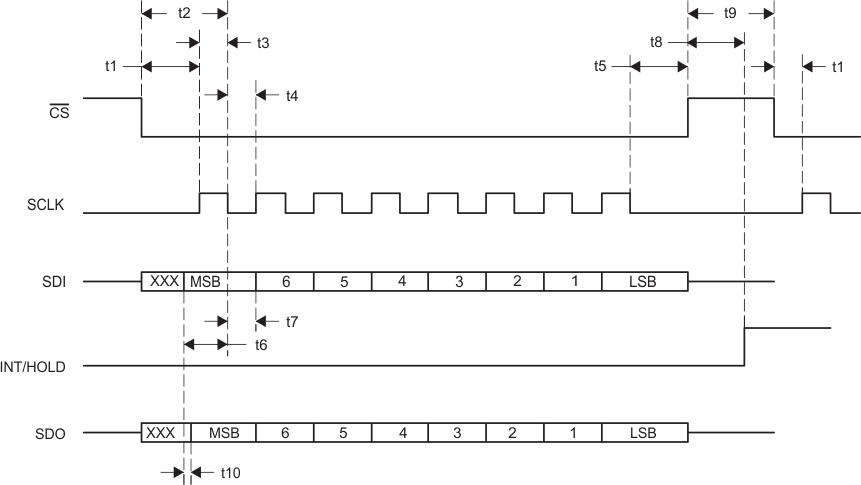
7.6 Timing Requirements
VDD = 5 V ±5%, TA = −40°C to 125°C (unless otherwise specified)| MIN | NOM | MAX | UNIT | ||
|---|---|---|---|---|---|
| ƒSPI | SPI frequency | 5 | MHz | ||
| t1 | Time from CS falling edge to SCLK rising edge | 10 | ns | ||
| t2 | Time from CS falling edge to SCLK falling edge | 80 | ns | ||
| t3 | Time for SCLK to go high | 60 | ns | ||
| t4 | Time for SCLK to go low | 60 | ns | ||
| t5 | Time from last SCLK falling edge to CS rising edge | 80 | ns | ||
| t6 | Time from SDI valid to falling edge of SCLK | 60 | ns | ||
| t7 | Time for SDI valid after falling edge of SCLK | 10 | ns | ||
| t8 | Time after CS rises until INT/HOLD to go high | 8 | ns | ||
| t9 | Time between two words for transmitting | 170 | ns | ||
| t10 | Time for SDO valid after SDI on bus, at VDD = 5 V and load = 20 pF | 40 | ns |
 Figure 1. Serial Peripheral Interface (SPI)
7.7 Typical Characteristics

