SLIS135E December 2010 – February 2017
PRODUCTION DATA.
- 1 Features
- 2 Applications
- 3 Description
- 4 Revision History
- 5 Pin Configuration and Functions
- 6 Specifications
- 7 Detailed Description
- 8 Application and Implementation
- 9 Power Supply Recommendations
- 10Layout
- 11Device and Documentation Support
- 12Mechanical, Packaging, and Orderable Information
パッケージ・オプション
メカニカル・データ(パッケージ|ピン)
- RTE|16
サーマルパッド・メカニカル・データ
- RTE|16
発注情報
7 Detailed Description
7.1 Overview
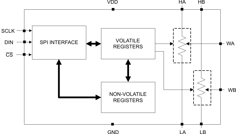
The TPL0202 has two linear-taper digital potentiometers with 256 wiper positions and an end-to-end resistance of 100 kΩ. Each potentiometer can be used as a three-terminal potentiometer or as a two-terminal rheostat. The two potentiometers can both be used in voltage divider mode or rheostat mode at the same time, or any combination of those modes. For example, potentiometer A can be used in voltage divider mode and potentiometer B can be used in rheostat mode. The two potentiometers are functionally independent of one another.
The high (H) and low (L) terminals of the TPL0202 are equivalent to the fixed terminals of a mechanical potentiometer. The H and L terminals do not have any polarity restrictions (H can be at a higher voltage than L, or L can be at a higher voltage than H). The position of the wiper (W) terminal is controlled by the value in the Wiper Resistance (WR) 8-bit register. When the WR register contains all zeroes (zero-scale), the wiper terminal is closest to its L terminal. As the value of the WR register increases from all zeroes to all ones (full-scale), the wiper moves from the position closest to the L terminal, to the position closest to the H terminal. At the same time, the resistance between W and L increases, whereas the resistance between W and H decreases.
The TPL0202 has non-volatile memory (EEPROM) that can be used to store the wiper position. When the device is powered down, the last value copied in the non-volatile memory (NVM) will be maintained. When power is restored, the contents of the NVM are automatically recalled and loaded into the corresponding wiper register to set the wipers. The internal registers of the TPL0202 can be written to using a SPI-compatible interface. The factory-programmed default value for the NVM is 0x80h (1000 0000). The wiper registers (volatile memory) and the NVM registers can be written to independently without having to modify the current value in another register. See the Register Map section for more information.
7.2 Functional Block Diagram
7.3 Feature Description
7.3.1 Dual Channel, 256-Position Resolution
The TPL0202 features two independent DPOTs. Each DPOT is capable of being used and controlled independently of the other one.
7.3.2 Non-Volatile Memory
The TPL0202 device features non-volatile memory which is used to store the wiper positions of both potentiometers independently. This allows the user to set the default power-up position of the wiper. By default, this is 0x80h (midscale).
7.4 Device Functional Modes
7.4.1 Voltage Divider Mode
The digital potentiometer generates a voltage divider when all three terminals are used. The voltage divider at wiper-to-H and wiper-to-L is proportional to the input voltage at H to L.
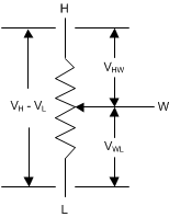 Figure 22. Equivalent Circuit for Voltage Divider Mode
For example, connecting terminal H to 5 V and terminal L to ground, the output voltage at terminal W can range from 0 V to 5 V. The general equation defining the output voltage at terminal W for any valid input voltage applied to terminal H and terminal L is:

The voltage difference between terminal H and terminal W can also be calculated using Equation 2.

where
- D is the decimal value of the wiper code.
7.4.2 Rheostat Mode
The TPL0202 operates in rheostat mode when only two terminals are used as a variable resistor. The variable resistance can either be between terminal H and terminal W or between terminal L and terminal W. The unused terminal can be left floating or it can be tied to terminal W. The nominal resistance between terminal H and terminal L is 10 kΩ and has 256 tap points accessed by the wiper terminal. The 8-bit volatile register value is used to determine one of the 256 possible wiper positions.
To set the resistance between terminal H and terminal W in rheostat mode, the potentiometer can be configured in two possible ways.
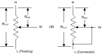 Figure 23. Equivalent Circuit for Rheostat Mode With Terminal H to Terminal W Resistance
The general equation for determining the digitally-programmed output resistance between terminal H and terminal W is:

where
- RTOT is the end-to-end resistance between terminal H and terminal L.
- D is the decimal value of the wiper code.
Similarly, to set the resistance between terminal L and terminal W, the potentiometer can be configured in two possible ways.
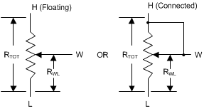 Figure 24. Equivalent Circuit for Rheostat Mode With Terminal L to Terminal W Resistance
The general equation for determining the digitally-programmed output resistance between terminal L and terminal W is:

where
- RTOT is the end-to-end resistance between terminal H and terminal L.
- D is the decimal value of the wiper code.
7.4.3 Ideal Resistance Values
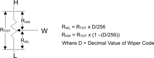 Figure 25. Digital Potentiometer Measurements
Table 1 shows the ideal values for DPOT with end-to-end resistance of 10 kΩ. The absolute values of resistance can vary significantly, but the ratio (RWL / RHW) is extremely accurate.
Table 1. Ideal Values for DPOT
| STEP | BINARY | HEX | 10 kΩ | RWL / RHW | |
|---|---|---|---|---|---|
| RWL | RHW | ||||
| 0 | 00000000 | 00 | 0.00 | 10.00 | 0.00 |
| 1 | 00000001 | 01 | 0.04 | 9.96 | 0.00 |
| 2 | 00000010 | 02 | 0.08 | 9.92 | 0.01 |
| 3 | 00000011 | 03 | 0.12 | 9.88 | 0.01 |
| 4 | 00000100 | 04 | 0.16 | 9.84 | 0.02 |
| 5 | 00000101 | 05 | 0.20 | 9.80 | 0.02 |
| 6 | 00000110 | 06 | 0.23 | 9.77 | 0.02 |
| 7 | 00000111 | 07 | 0.27 | 9.73 | 0.03 |
| 8 | 00001000 | 08 | 0.31 | 9.69 | 0.03 |
| 9 | 00001001 | 09 | 0.35 | 9.65 | 0.04 |
| 10 | 00001010 | 0A | 0.39 | 9.61 | 0.04 |
| 11 | 00001011 | 0B | 0.43 | 9.57 | 0.04 |
| 12 | 00001100 | 0C | 0.47 | 9.53 | 0.05 |
| 13 | 00001101 | 0D | 0.51 | 9.49 | 0.05 |
| 14 | 00001110 | 0E | 0.55 | 9.45 | 0.06 |
| 15 | 00001111 | 0F | 0.59 | 9.41 | 0.06 |
| 16 | 00010000 | 10 | 0.63 | 9.38 | 0.07 |
| 17 | 00010001 | 11 | 0.66 | 9.34 | 0.07 |
| 18 | 00010010 | 12 | 0.70 | 9.30 | 0.08 |
| 19 | 00010011 | 13 | 0.74 | 9.26 | 0.08 |
| 20 | 00010100 | 14 | 0.78 | 9.22 | 0.08 |
| 21 | 00010101 | 15 | 0.82 | 9.18 | 0.09 |
| 22 | 00010110 | 16 | 0.86 | 9.14 | 0.09 |
| 23 | 00010111 | 17 | 0.90 | 9.10 | 0.10 |
| 24 | 00011000 | 18 | 0.94 | 9.06 | 0.10 |
| 25 | 00011001 | 19 | 0.98 | 9.02 | 0.11 |
| 26 | 00011010 | 1A | 1.02 | 8.98 | 0.11 |
| 27 | 00011011 | 1B | 1.05 | 8.95 | 0.12 |
| 28 | 00011100 | 1C | 1.09 | 8.91 | 0.12 |
| 29 | 00011101 | 1D | 1.13 | 8.87 | 0.13 |
| 30 | 00011110 | 1E | 1.17 | 8.83 | 0.13 |
| 31 | 00011111 | 1F | 1.21 | 8.79 | 0.14 |
| 32 | 00100000 | 20 | 1.25 | 8.75 | 0.14 |
| 33 | 00100001 | 21 | 1.29 | 8.71 | 0.15 |
| 34 | 00100010 | 22 | 1.33 | 8.67 | 0.15 |
| 35 | 00100011 | 23 | 1.37 | 8.63 | 0.16 |
| 36 | 00100100 | 24 | 1.41 | 8.59 | 0.16 |
| 37 | 00100101 | 25 | 1.45 | 8.55 | 0.17 |
| 38 | 00100110 | 26 | 1.48 | 8.52 | 0.17 |
| 39 | 00100111 | 27 | 1.52 | 8.48 | 0.18 |
| 40 | 00101000 | 28 | 1.56 | 8.44 | 0.19 |
| 41 | 00101001 | 29 | 1.60 | 8.40 | 0.19 |
| 42 | 00101010 | 2A | 1.64 | 8.36 | 0.20 |
| 43 | 00101011 | 2B | 1.68 | 8.32 | 0.20 |
| 44 | 00101100 | 2C | 1.72 | 8.28 | 0.21 |
| 45 | 00101101 | 2D | 1.76 | 8.24 | 0.21 |
| 46 | 00101110 | 2E | 1.80 | 8.20 | 0.22 |
| 47 | 00101111 | 2F | 1.84 | 8.16 | 0.22 |
| 48 | 00110000 | 30 | 1.88 | 8.13 | 0.23 |
| 49 | 00110001 | 31 | 1.91 | 8.09 | 0.24 |
| 50 | 00110010 | 32 | 1.95 | 8.05 | 0.24 |
| 51 | 00110011 | 33 | 1.99 | 8.01 | 0.25 |
| 52 | 00110100 | 34 | 2.03 | 7.97 | 0.25 |
| 53 | 00110101 | 35 | 2.07 | 7.93 | 0.26 |
| 54 | 00110110 | 36 | 2.11 | 7.89 | 0.27 |
| 55 | 00110111 | 37 | 2.15 | 7.85 | 0.27 |
| 56 | 00111000 | 38 | 2.19 | 7.81 | 0.28 |
| 57 | 00111001 | 39 | 2.23 | 7.77 | 0.29 |
| 58 | 00111010 | 3A | 2.27 | 7.73 | 0.29 |
| 59 | 00111011 | 3B | 2.30 | 7.70 | 0.30 |
| 60 | 00111100 | 3C | 2.34 | 7.66 | 0.31 |
| 61 | 00111101 | 3D | 2.38 | 7.62 | 0.31 |
| 62 | 00111110 | 3E | 2.42 | 7.58 | 0.32 |
| 63 | 00111111 | 3F | 2.46 | 7.54 | 0.33 |
| 64 | 01000000 | 40 | 2.50 | 7.50 | 0.33 |
| 65 | 01000001 | 41 | 2.54 | 7.46 | 0.34 |
| 66 | 01000010 | 42 | 2.58 | 7.42 | 0.35 |
| 67 | 01000011 | 43 | 2.62 | 7.38 | 0.35 |
| 68 | 01000100 | 44 | 2.66 | 7.34 | 0.36 |
| 69 | 01000101 | 45 | 2.70 | 7.30 | 0.37 |
| 70 | 01000110 | 46 | 2.73 | 7.27 | 0.38 |
| 71 | 01000111 | 47 | 2.77 | 7.23 | 0.38 |
| 72 | 01001000 | 48 | 2.81 | 7.19 | 0.39 |
| 73 | 01001001 | 49 | 2.85 | 7.15 | 0.40 |
| 74 | 01001010 | 4A | 2.89 | 7.11 | 0.41 |
| 75 | 01001011 | 4B | 2.93 | 7.07 | 0.41 |
| 76 | 01001100 | 4C | 2.97 | 7.03 | 0.42 |
| 77 | 01001101 | 4D | 3.01 | 6.99 | 0.43 |
| 78 | 01001110 | 4E | 3.05 | 6.95 | 0.44 |
| 79 | 01001111 | 4F | 3.09 | 6.91 | 0.45 |
| 80 | 01010000 | 50 | 3.13 | 6.88 | 0.45 |
| 81 | 01010001 | 51 | 3.16 | 6.84 | 0.46 |
| 82 | 01010010 | 52 | 3.20 | 6.80 | 0.47 |
| 83 | 01010011 | 53 | 3.24 | 6.76 | 0.48 |
| 84 | 01010100 | 54 | 3.28 | 6.72 | 0.49 |
| 85 | 01010101 | 55 | 3.32 | 6.68 | 0.50 |
| 86 | 01010110 | 56 | 3.36 | 6.64 | 0.51 |
| 87 | 01010111 | 57 | 3.40 | 6.60 | 0.51 |
| 88 | 01011000 | 58 | 3.44 | 6.56 | 0.52 |
| 89 | 01011001 | 59 | 3.48 | 6.52 | 0.53 |
| 90 | 01011010 | 5A | 3.52 | 6.48 | 0.54 |
| 91 | 01011011 | 5B | 3.55 | 6.45 | 0.55 |
| 92 | 01011100 | 5C | 3.59 | 6.41 | 0.56 |
| 93 | 01011101 | 5D | 3.63 | 6.37 | 0.57 |
| 94 | 01011110 | 5E | 3.67 | 6.33 | 0.58 |
| 95 | 01011111 | 5F | 3.71 | 6.29 | 0.59 |
| 96 | 01100000 | 60 | 3.75 | 6.25 | 0.60 |
| 97 | 01100001 | 61 | 3.79 | 6.21 | 0.61 |
| 98 | 01100010 | 62 | 3.83 | 6.17 | 0.62 |
| 99 | 01100011 | 63 | 3.87 | 6.13 | 0.63 |
| 100 | 01100100 | 64 | 3.91 | 6.09 | 0.64 |
| 101 | 01100101 | 65 | 3.95 | 6.05 | 0.65 |
| 102 | 01100110 | 66 | 3.98 | 6.02 | 0.66 |
| 103 | 01100111 | 67 | 4.02 | 5.98 | 0.67 |
| 104 | 01101000 | 68 | 4.06 | 5.94 | 0.68 |
| 105 | 01101001 | 69 | 4.10 | 5.90 | 0.70 |
| 106 | 01101010 | 6A | 4.14 | 5.86 | 0.71 |
| 107 | 01101011 | 6B | 4.18 | 5.82 | 0.72 |
| 108 | 01101100 | 6C | 4.22 | 5.78 | 0.73 |
| 109 | 01101101 | 6D | 4.26 | 5.74 | 0.74 |
| 110 | 01101110 | 6E | 4.30 | 5.70 | 0.75 |
| 111 | 01101111 | 6F | 4.34 | 5.66 | 0.77 |
| 112 | 01110000 | 70 | 4.38 | 5.63 | 0.78 |
| 113 | 01110001 | 71 | 4.41 | 5.59 | 0.79 |
| 114 | 01110010 | 72 | 4.45 | 5.55 | 0.80 |
| 115 | 01110011 | 73 | 4.49 | 5.51 | 0.82 |
| 116 | 01110100 | 74 | 4.53 | 5.47 | 0.83 |
| 117 | 01110101 | 75 | 4.57 | 5.43 | 0.84 |
| 118 | 01110110 | 76 | 4.61 | 5.39 | 0.86 |
| 119 | 01110111 | 77 | 4.65 | 5.35 | 0.87 |
| 120 | 01111000 | 78 | 4.69 | 5.31 | 0.88 |
| 121 | 01111001 | 79 | 4.73 | 5.27 | 0.90 |
| 122 | 01111010 | 7A | 4.77 | 5.23 | 0.91 |
| 123 | 01111011 | 7B | 4.80 | 5.20 | 0.92 |
| 124 | 01111100 | 7C | 4.84 | 5.16 | 0.94 |
| 125 | 01111101 | 7D | 4.88 | 5.12 | 0.95 |
| 126 | 01111110 | 7E | 4.92 | 5.08 | 0.97 |
| 127 | 01111111 | 7F | 4.96 | 5.04 | 0.98 |
| 128 | 10000000 | 80 | 5.00 | 5.00 | 1.00 |
| 129 | 10000001 | 81 | 5.04 | 4.96 | 1.02 |
| 130 | 10000010 | 82 | 5.08 | 4.92 | 1.03 |
| 131 | 10000011 | 83 | 5.12 | 4.88 | 1.05 |
| 132 | 10000100 | 84 | 5.16 | 4.84 | 1.06 |
| 133 | 10000101 | 85 | 5.20 | 4.80 | 1.08 |
| 134 | 10000110 | 86 | 5.23 | 4.77 | 1.10 |
| 135 | 10000111 | 87 | 5.27 | 4.73 | 1.12 |
| 136 | 10001000 | 88 | 5.31 | 4.69 | 1.13 |
| 137 | 10001001 | 89 | 5.35 | 4.65 | 1.15 |
| 138 | 10001010 | 8A | 5.39 | 4.61 | 1.17 |
| 139 | 10001011 | 8B | 5.43 | 4.57 | 1.19 |
| 140 | 10001100 | 8C | 5.47 | 4.53 | 1.21 |
| 141 | 10001101 | 8D | 5.51 | 4.49 | 1.23 |
| 142 | 10001110 | 8E | 5.55 | 4.45 | 1.25 |
| 143 | 10001111 | 8F | 5.59 | 4.41 | 1.27 |
| 144 | 10010000 | 90 | 5.63 | 4.38 | 1.29 |
| 145 | 10010001 | 91 | 5.66 | 4.34 | 1.31 |
| 146 | 10010010 | 92 | 5.70 | 4.30 | 1.33 |
| 147 | 10010011 | 93 | 5.74 | 4.26 | 1.35 |
| 148 | 10010100 | 94 | 5.78 | 4.22 | 1.37 |
| 149 | 10010101 | 95 | 5.82 | 4.18 | 1.39 |
| 150 | 10010110 | 96 | 5.86 | 4.14 | 1.42 |
| 151 | 10010111 | 97 | 5.90 | 4.10 | 1.44 |
| 152 | 10011000 | 98 | 5.94 | 4.06 | 1.46 |
| 153 | 10011001 | 99 | 5.98 | 4.02 | 1.49 |
| 154 | 10011010 | 9A | 6.02 | 3.98 | 1.51 |
| 155 | 10011011 | 9B | 6.05 | 3.95 | 1.53 |
| 156 | 10011100 | 9C | 6.09 | 3.91 | 1.56 |
| 157 | 10011101 | 9D | 6.13 | 3.87 | 1.59 |
| 158 | 10011110 | 9E | 6.17 | 3.83 | 1.61 |
| 159 | 10011111 | 9F | 6.21 | 3.79 | 1.64 |
| 160 | 10100000 | A0 | 6.25 | 3.75 | 1.67 |
| 161 | 10100001 | A1 | 6.29 | 3.71 | 1.69 |
| 162 | 10100010 | A2 | 6.33 | 3.67 | 1.72 |
| 163 | 10100011 | A3 | 6.37 | 3.63 | 1.75 |
| 164 | 10100100 | A4 | 6.41 | 3.59 | 1.78 |
| 165 | 10100101 | A5 | 6.45 | 3.55 | 1.81 |
| 166 | 10100110 | A6 | 6.48 | 3.52 | 1.84 |
| 167 | 10100111 | A7 | 6.52 | 3.48 | 1.88 |
| 168 | 10101000 | A8 | 6.56 | 3.44 | 1.91 |
| 169 | 10101001 | A9 | 6.60 | 3.40 | 1.94 |
| 170 | 10101010 | AA | 6.64 | 3.36 | 1.98 |
| 171 | 10101011 | AB | 6.68 | 3.32 | 2.01 |
| 172 | 10101100 | AC | 6.72 | 3.28 | 2.05 |
| 173 | 10101101 | AD | 6.76 | 3.24 | 2.08 |
| 174 | 10101110 | AE | 6.80 | 3.20 | 2.12 |
| 175 | 10101111 | AF | 6.84 | 3.16 | 2.16 |
| 176 | 10110000 | B0 | 6.88 | 3.13 | 2.20 |
| 177 | 10110001 | B1 | 6.91 | 3.09 | 2.24 |
| 178 | 10110010 | B2 | 6.95 | 3.05 | 2.28 |
| 179 | 10110011 | B3 | 6.99 | 3.01 | 2.32 |
| 180 | 10110100 | B4 | 7.03 | 2.97 | 2.37 |
| 181 | 10110101 | B5 | 7.07 | 2.93 | 2.41 |
| 182 | 10110110 | B6 | 7.11 | 2.89 | 2.46 |
| 183 | 10110111 | B7 | 7.15 | 2.85 | 2.51 |
| 184 | 10111000 | B8 | 7.19 | 2.81 | 2.56 |
| 185 | 10111001 | B9 | 7.23 | 2.77 | 2.61 |
| 186 | 10111010 | BA | 7.27 | 2.73 | 2.66 |
| 187 | 10111011 | BB | 7.30 | 2.70 | 2.71 |
| 188 | 10111100 | BC | 7.34 | 2.66 | 2.76 |
| 189 | 10111101 | BD | 7.38 | 2.62 | 2.82 |
| 190 | 10111110 | BE | 7.42 | 2.58 | 2.88 |
| 191 | 10111111 | BF | 7.46 | 2.54 | 2.94 |
| 192 | 11000000 | C0 | 7.50 | 2.50 | 3.00 |
| 193 | 11000001 | C1 | 7.54 | 2.46 | 3.06 |
| 194 | 11000010 | C2 | 7.58 | 2.42 | 3.13 |
| 195 | 11000011 | C3 | 7.62 | 2.38 | 3.20 |
| 196 | 11000100 | C4 | 7.66 | 2.34 | 3.27 |
| 197 | 11000101 | C5 | 7.70 | 2.30 | 3.34 |
| 198 | 11000110 | C6 | 7.73 | 2.27 | 3.41 |
| 199 | 11000111 | C7 | 7.77 | 2.23 | 3.49 |
| 200 | 11001000 | C8 | 7.81 | 2.19 | 3.57 |
| 201 | 11001001 | C9 | 7.85 | 2.15 | 3.65 |
| 202 | 11001010 | CA | 7.89 | 2.11 | 3.74 |
| 203 | 11001011 | CB | 7.93 | 2.07 | 3.83 |
| 204 | 11001100 | CC | 7.97 | 2.03 | 3.92 |
| 205 | 11001101 | CD | 8.01 | 1.99 | 4.02 |
| 206 | 11001110 | CE | 8.05 | 1.95 | 4.12 |
| 207 | 11001111 | CF | 8.09 | 1.91 | 4.22 |
| 208 | 11010000 | D0 | 8.13 | 1.88 | 4.33 |
| 209 | 11010001 | D1 | 8.16 | 1.84 | 4.45 |
| 210 | 11010010 | D2 | 8.20 | 1.80 | 4.57 |
| 211 | 11010011 | D3 | 8.24 | 1.76 | 4.69 |
| 212 | 11010100 | D4 | 8.28 | 1.72 | 4.82 |
| 213 | 11010101 | D5 | 8.32 | 1.68 | 4.95 |
| 214 | 11010110 | D6 | 8.36 | 1.64 | 5.10 |
| 215 | 11010111 | D7 | 8.40 | 1.60 | 5.24 |
| 216 | 11011000 | D8 | 8.44 | 1.56 | 5.40 |
| 217 | 11011001 | D9 | 8.48 | 1.52 | 5.56 |
| 218 | 11011010 | DA | 8.52 | 1.48 | 5.74 |
| 219 | 11011011 | DB | 8.55 | 1.45 | 5.92 |
| 220 | 11011100 | DC | 8.59 | 1.41 | 6.11 |
| 221 | 11011101 | DD | 8.63 | 1.37 | 6.31 |
| 222 | 11011110 | DE | 8.67 | 1.33 | 6.53 |
| 223 | 11011111 | DF | 8.71 | 1.29 | 6.76 |
| 224 | 11100000 | E0 | 8.75 | 1.25 | 7.00 |
| 225 | 11100001 | E1 | 8.79 | 1.21 | 7.26 |
| 226 | 11100010 | E2 | 8.83 | 1.17 | 7.53 |
| 227 | 11100011 | E3 | 8.87 | 1.13 | 7.83 |
| 228 | 11100100 | E4 | 8.91 | 1.09 | 8.14 |
| 229 | 11100101 | E5 | 8.95 | 1.05 | 8.48 |
| 230 | 11100110 | E6 | 8.98 | 1.02 | 8.85 |
| 231 | 11100111 | E7 | 9.02 | 0.98 | 9.24 |
| 232 | 11101000 | E8 | 9.06 | 0.94 | 9.67 |
| 233 | 11101001 | E9 | 9.10 | 0.90 | 10.13 |
| 234 | 11101010 | EA | 9.14 | 0.86 | 10.64 |
| 235 | 11101011 | EB | 9.18 | 0.82 | 11.19 |
| 236 | 11101100 | EC | 9.22 | 0.78 | 11.80 |
| 237 | 11101101 | ED | 9.26 | 0.74 | 12.47 |
| 238 | 11101110 | EE | 9.30 | 0.70 | 13.22 |
| 239 | 11101111 | EF | 9.34 | 0.66 | 14.06 |
| 240 | 11110000 | F0 | 9.38 | 0.63 | 15.00 |
| 241 | 11110001 | F1 | 9.41 | 0.59 | 16.07 |
| 242 | 11110010 | F2 | 9.45 | 0.55 | 17.29 |
| 243 | 11110011 | F3 | 9.49 | 0.51 | 18.69 |
| 244 | 11110100 | F4 | 9.53 | 0.47 | 20.33 |
| 245 | 11110101 | F5 | 9.57 | 0.43 | 22.27 |
| 246 | 11110110 | F6 | 9.61 | 0.39 | 24.60 |
| 247 | 11110111 | F7 | 9.65 | 0.35 | 27.44 |
| 248 | 11111000 | F8 | 9.69 | 0.31 | 31.00 |
| 249 | 11111001 | F9 | 9.73 | 0.27 | 35.57 |
| 250 | 11111010 | FA | 9.77 | 0.23 | 41.67 |
| 251 | 11111011 | FB | 9.80 | 0.20 | 50.20 |
| 252 | 11111100 | FC | 9.84 | 0.16 | 63.00 |
| 253 | 11111101 | FD | 9.88 | 0.12 | 84.33 |
| 254 | 11111110 | FE | 9.92 | 0.08 | 127.00 |
| 255 | 11111111 | FF | 9.96 | 0.04 | 255.00 |
7.5 Programming
7.5.1 SPI Digital Interface
The TPL0202 uses a 3-wire SPI-compatible serial data interface. This write-only interface has three inputs: chip-select (CS), data clock (SCLK), and data input (DIN). Drive CS low to enable the serial interface and clock data synchronously into the shift register on each SCLK rising edge. The WRITE commands (C1, C0 = 00 or 01) require 16 clock cycles to clock in the command, address, and data. The COPY commands (C1, C0 = 10 or 11) can use either eight clock cycles to transfer only command and address bits or 16 clock cycles, with the device disregarding 8 data bits. After loading data into the shift register, drive CS high to latch the data into the appropriate potentiometer control register and disable the serial interface. Keep CS low during the entire serial data stream to avoid corruption of the data.
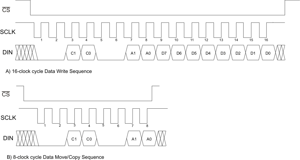 Figure 26. Digital Interface Write Sequence
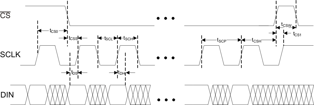 Figure 27. Digital Interface Timing Diagram
7.6 Register Map
Table 2. Register Map
| CLOCK EDGE | 1 | 2 | 3 | 4 | 5 | 6 | 7 | 8 | 9 | 10 | 11 | 12 | 13 | 14 | 15 | 16 |
|---|---|---|---|---|---|---|---|---|---|---|---|---|---|---|---|---|
| – | – | C1 | C0 | – | – | A1 | A0 | D7 | D6 | D5 | D4 | D3 | D2 | D1 | D0 | |
| Write Wiper Register A | 0 | 0 | 0 | 0 | 0 | 0 | 0 | 1 | D7 | D6 | D5 | D4 | D3 | D2 | D1 | D0 |
| Write Wiper Register B | 0 | 0 | 0 | 0 | 0 | 0 | 1 | 0 | D7 | D6 | D5 | D4 | D3 | D2 | D1 | D0 |
| Write Wiper Register A and B | 0 | 0 | 0 | 0 | 0 | 0 | 1 | 1 | D7 | D6 | D5 | D4 | D3 | D2 | D1 | D0 |
| Write NV Register A | 0 | 0 | 0 | 1 | 0 | 0 | 0 | 1 | D7 | D6 | D5 | D4 | D3 | D2 | D1 | D0 |
| Write NV Register B | 0 | 0 | 0 | 1 | 0 | 0 | 1 | 0 | D7 | D6 | D5 | D4 | D3 | D2 | D1 | D0 |
| Write NV Register A and B | 0 | 0 | 0 | 1 | 0 | 0 | 1 | 1 | D7 | D6 | D5 | D4 | D3 | D2 | D1 | D0 |
| Copy Wiper Register A to NV Register A | 0 | 0 | 1 | 0 | 0 | 0 | 0 | 1 | – | – | – | – | – | – | – | – |
| Copy Wiper Register B to NV Register B | 0 | 0 | 1 | 0 | 0 | 0 | 1 | 0 | – | – | – | – | – | – | – | – |
| Copy Both Wiper Registers to NV Registers | 0 | 0 | 1 | 0 | 0 | 0 | 1 | 1 | – | – | – | – | – | – | – | – |
| Copy NV Register A to Wiper Register A | 0 | 0 | 1 | 1 | 0 | 0 | 0 | 1 | – | – | – | – | – | – | – | – |
| Copy NV Register B to Wiper Register A | 0 | 0 | 1 | 1 | 0 | 0 | 1 | 0 | – | – | – | – | – | – | – | – |
| Copy Both NV Registers to Wiper Registers | 0 | 0 | 1 | 1 | 0 | 0 | 1 | 1 | – | – | – | – | – | – | – | – |
7.6.1 Digital Interface Format
The data format consists of three elements: command bits, address bits, and data bits. The command bits (C1 and C0) indicate the action to be taken such as changing or storing the wiper position. The address bits (A1 and A0) specify which potentiometer the command affects and the 8 data bits (D7 to D0) specify the wiper position.
7.6.2 Write-Wiper Register (Command 00)
Data written to the write-wiper registers (C1, C0 = 00) controls the wiper positions. The 8 data bits (D7 to D0) indicate the position of the wiper. If DIN = 0x00h, the wiper moves to the position closest to the L terminal. If DIN = 0xFFh, the wiper moves to the position closest to the H terminal. This command writes data to the volatile RAM, leaving the NV registers unchanged. When the device powers up, the data stored in the NV registers transfers to the volatile wiper register, moving the wiper to the stored position
7.6.3 Write-NV Register (Command 01)
This command (C1, C0 = 01) stores the position of the wipers to the NV registers for use at power-up. Alternatively, the copy wiper register to NV register command can be used to store the position of the wipers to the NV registers. Writing to the NV registers does not affect the position of the wipers.
7.6.4 Copy Wiper Register to NV Register (Command 10)
This command (C1, C0 = 10) stores the current position of the wiper to the NV register, for use at power-up. This command may affect one potentiometer at a time, or both simultaneously, depending on the state of A1 and A0. Alternatively, the write NV register command can be used to store the current position of the wiper to the NV register.
7.6.5 Copy NV Register to Wiper Register (Command 11)
This command (C1, C0 = 11) restores the wiper position to the previously stored position in the NV register. This command may affect one potentiometer at a time, or both simultaneously, depending on the state of A1 and A0.