SLIS144B September   2011  – February 2017

PRODUCTION DATA.  

  1. Features
  2. Applications
  3. Description
  4. Revision History
  5. Device Comparison Table
  6. Pin Configuration and Functions
  7. Specifications
    1. 7.1 Absolute Maximum Ratings
    2. 7.2 ESD Ratings
    3. 7.3 Recommended Operating Conditions
    4. 7.4 Thermal Information
    5. 7.5 Electrical Characteristics
    6. 7.6 Timing Requirements
    7. 7.7 Typical Characteristics
  8. Parameter Measurement Information
  9. Detailed Description
    1. 9.1 Overview
    2. 9.2 Functional Block Diagram
    3. 9.3 Feature Description
    4. 9.4 Device Functional Modes
      1. 9.4.1 Voltage Divider Mode
    5. 9.5 Programming
      1. 9.5.1 I2C General Operation and Overview
        1. 9.5.1.1 START and STOP Conditions
        2. 9.5.1.2 Data Validity and Byte Formation
        3. 9.5.1.3 Acknowledge (ACK) and Not Acknowledge (NACK)
        4. 9.5.1.4 Repeated Start
      2. 9.5.2 Programing with I2C
        1. 9.5.2.1 Write Operation
        2. 9.5.2.2 Read Operation
    6. 9.6 Register Maps
      1. 9.6.1 Slave Address
      2. 9.6.2 Register Address
  10. 10Application and Implementation
    1. 10.1 Application Information
    2. 10.2 Typical Application
      1. 10.2.1 Design Requirements
      2. 10.2.2 Detailed Design Procedure
      3. 10.2.3 Application Curve
  11. 11Power Supply Recommendations
    1. 11.1 Power Sequence
    2. 11.2 Power-On Reset Requirements
    3. 11.3 I2C Communication After Power Up
    4. 11.4 Wiper Position While Unpowered and After Power Up
  12. 12Layout
    1. 12.1 Layout Guidelines
    2. 12.2 Layout Example
  13. 13Device and Documentation Support
    1. 13.1 Documentation Support
      1. 13.1.1 Related Documentation
    2. 13.2 Related Links
    3. 13.3 Receiving Notification of Documentation Updates
    4. 13.4 Community Resources
    5. 13.5 Trademarks
    6. 13.6 Electrostatic Discharge Caution
    7. 13.7 Glossary
  14. 14Mechanical, Packaging, and Orderable Information

パッケージ・オプション

メカニカル・データ(パッケージ|ピン)
サーマルパッド・メカニカル・データ
発注情報

Layout

Layout Guidelines

To ensure reliability of the device, follow common printed-circuit board (PCB) layout guidelines:

  • Leads to the input must be as direct as possible with a minimum conductor length.
  • The ground path must have low resistance and low inductance.
  • Use short trace-lengths to avoid excessive loading.
  • It is common to have a dedicated ground plane on an inner layer of the board.
  • Terminals that are connected to ground must have a low-impedance path to the ground plane in the form of wide polygon pours and multiple vias.
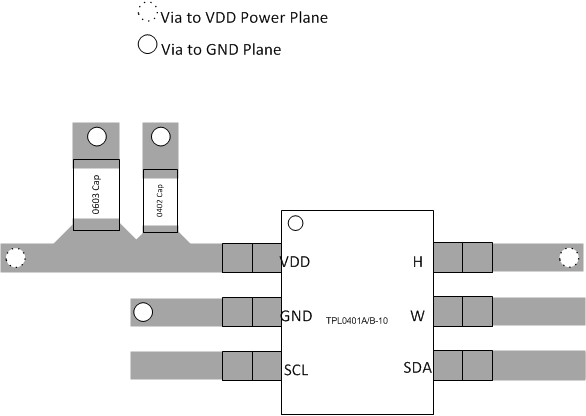
  • Use bypass capacitors on power supplies and placed them as close as possible to the VDD pin.
  • Apply low equivalent series resistance (0.1-μF to 10-μF tantalum or electrolytic capacitors) at the supplies to minimize transient disturbances and to filter low-frequency ripple.
  • To reduce the total I2C bus capacitance added by PCB parasitics, data lines (SCL and SDA) must be as short as possible and the widths of the traces must also be minimized (for example, 5 to 10 mils depending on copper weight).

Layout Example

TPL0401A TPL0401B Layout_SLIS144.gif Figure 24. Layout Recommendation