SLIS144B September 2011 – February 2017
PRODUCTION DATA.
- 1 Features
- 2 Applications
- 3 Description
- 4 Revision History
- 5 Device Comparison Table
- 6 Pin Configuration and Functions
- 7 Specifications
- 8 Parameter Measurement Information
- 9 Detailed Description
- 10Application and Implementation
- 11Power Supply Recommendations
- 12Layout
- 13Device and Documentation Support
- 14Mechanical, Packaging, and Orderable Information
11 Power Supply Recommendations
11.1 Power Sequence
Protection diodes limit the voltage compliance at SDA, SCL, terminal H, and terminal W, making it important to power up VDD first before applying any voltage to SDA, SCL, terminal H, and terminal W. The diodes are forward-biasing, meaning VDD can be powered unintentionally if VDD is not powered first. The ideal power-up sequence is VDD, digital inputs, and VW and VH. The order of powering digital inputs, VH and VW does not matter as long as they are powered after VDD.
11.2 Power-On Reset Requirements
In the event of a glitch or data corruption, the TPL0401-10 can be reset to its default conditions by using the power-on reset feature. Power-on reset requires that the device go through a power cycle to be completely reset. This reset also happens when the device is powered on for the first time in an application.
 Figure 22. VDD is Lowered to 0 V and then Ramped Up to VDD
Table 4 specifies the performance of the power-on reset feature for the TPL0401-10 for both types of power-on reset.
11.3 I2C Communication After Power Up
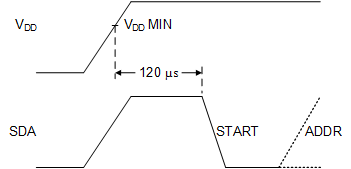
In order to ensure a complete device reset after a power up condition, the user must wait 120 µs after power up before initiating communication with the TPL0401x-10. See Figure 23 for an example waveform.
 Figure 23. Recommended Start Up Sequence
11.4 Wiper Position While Unpowered and After Power Up
When DPOT is powered off, the impedance of the device is undefined and not known.
Upon power-up, the device returns to 0×40h code because this device does not contain non-volatile memory.