JAJSG89A January   2015  – September 2018 TPL5010

PRODUCTION DATA.  

  1. 特長
  2. アプリケーション
  3. 概要
    1.     Device Images
      1.      簡略化されたアプリケーション回路図
  4. 改訂履歴
  5. デバイス比較表
  6. Pin Configuration and Functions
    1.     Pin Functions
  7. Specifications
    1. 7.1 Absolute Maximum Ratings
    2. 7.2 ESD Ratings
    3. 7.3 Recommended Operating Ratings
    4. 7.4 Thermal Information
    5. 7.5 Electrical Characteristics
    6. 7.6 Timing Requirements
    7. 7.7 Typical Characteristics
  8. Detailed Description
    1. 8.1 Overview
    2. 8.2 Functional Block Diagram
    3. 8.3 Feature Description
      1. 8.3.1 WAKE
      2. 8.3.2 DONE
      3. 8.3.3 RSTn
    4. 8.4 Device Functional Modes
      1. 8.4.1 Start-Up
      2. 8.4.2 Normal Operating Mode
    5. 8.5 Programming
      1. 8.5.1 Configuring the WAKE Interval With the DELAY/M_RST Pin
      2. 8.5.2 Manual Reset
        1. 8.5.2.1 DELAY/M_RST
        2. 8.5.2.2 Circuitry
      3. 8.5.3 Timer Interval Selection Using External Resistance
      4. 8.5.4 Quantization Error
      5. 8.5.5 Error Due to Real External Resistance
  9. Application and Implementation
    1. 9.1 Application Information
    2. 9.2 Typical Application
      1. 9.2.1 Design Requirements
      2. 9.2.2 Detailed Design Procedure
      3. 9.2.3 Application Curve
  10. 10Power Supply Recommendations
  11. 11Layout
    1. 11.1 Layout Guidelines
    2. 11.2 Layout Example
  12. 12デバイスおよびドキュメントのサポート
    1. 12.1 ドキュメントの更新通知を受け取る方法
    2. 12.2 コミュニティ・リソース
    3. 12.3 商標
    4. 12.4 静電気放電に関する注意事項
    5. 12.5 Glossary
  13. 13メカニカル、パッケージ、および注文情報

パッケージ・オプション

メカニカル・データ(パッケージ|ピン)
サーマルパッド・メカニカル・データ
発注情報

Pin Configuration and Functions

DDC Package
6-Lead SOT-23
Top View
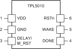
TPL5010 PIN_OUT_5010.gif

Pin Functions

PIN TYPE(1) DESCRIPTION APPLICATION INFORMATION
NO. NAME
1 VDD P Supply voltage
2 GND G Ground
3 DELAY/ M_RST I Time Interval set and Manual Reset Resistance between this pin and GND is used to select the time interval. The reset switch is also connected to this pin.
4 DONE I Logic Input for watchdog functionality Digital signal driven by the µC to indicate successful processing of the WAKE signal.
5 WAKE O Timer output signal generated every tIP period. Digital pulsed signal to wake up the µC at the end of the programmed time interval.
6 RSTn O Reset Output (open drain output) Digital signal to RESET the µC, pullup resistance is required
G= Ground, P= Power, O= Output, I= Input.