SLVSE16C May   2019  – January  2020 TPS1HB08-Q1

PRODUCTION DATA.  

  1. Features
  2. Applications
  3. Description
    1.     Simplified Schematic
  4. Revision History
  5. Device Comparison Table
  6. Pin Configuration and Functions
    1.     Pin Functions
    2. 6.1 Recommended Connections for Unused Pins
  7. Specifications
    1. Table 3. Absolute Maximum Ratings
    2. Table 4. ESD Ratings
    3. Table 5. Recommended Operating Conditions
    4. Table 6. Thermal Information
    5. Table 7. Electrical Characteristics
    6. Table 8. SNS Timing Characteristics
    7. Table 9. Switching Characteristics
    8. 7.1      Typical Characteristics
  8. Parameter Measurement Information
  9. Detailed Description
    1. 9.1 Overview
    2. 9.2 Functional Block Diagram
    3. 9.3 Feature Description
      1. 9.3.1 Protection Mechanisms
        1. 9.3.1.1 Thermal Shutdown
        2. 9.3.1.2 Current Limit
          1. 9.3.1.2.1 Current Limit Foldback
          2. 9.3.1.2.2 Programmable Current Limit
          3. 9.3.1.2.3 Undervoltage Lockout (UVLO)
          4. 9.3.1.2.4 VBB During Short-to-Ground
        3. 9.3.1.3 Voltage Transients
          1. 9.3.1.3.1 Load Dump
          2. 9.3.1.3.2 Driving Inductive Loads
        4. 9.3.1.4 Reverse Battery
        5. 9.3.1.5 Fault Event – Timing Diagrams - Version A and B
        6. 9.3.1.6 Fault Event – Timing Diagrams - Version F
      2. 9.3.2 Diagnostic Mechanisms
        1. 9.3.2.1 VOUT Short-to-Battery and Open-Load
          1. 9.3.2.1.1 Detection With Switch Enabled
          2. 9.3.2.1.2 Detection With Switch Disabled
        2. 9.3.2.2 SNS Output
          1. 9.3.2.2.1 RSNS Value
            1. 9.3.2.2.1.1 High Accuracy Load Current Sense
            2. 9.3.2.2.1.2 SNS Output Filter
        3. 9.3.2.3 Fault Indication and SNS Mux
        4. 9.3.2.4 Resistor Sharing
        5. 9.3.2.5 High-Frequency, Low Duty-Cycle Current Sensing
    4. 9.4 Device Functional Modes
      1. 9.4.1 Off
      2. 9.4.2 Standby
      3. 9.4.3 Diagnostic
      4. 9.4.4 Standby Delay
      5. 9.4.5 Active
      6. 9.4.6 Fault
  10. 10Application and Implementation
    1. 10.1 Application Information
      1. 10.1.1 Ground Protection Network
      2. 10.1.2 Interface With Microcontroller
      3. 10.1.3 I/O Protection
      4. 10.1.4 Inverse Current
      5. 10.1.5 Loss of GND
      6. 10.1.6 Automotive Standards
        1. 10.1.6.1 ISO7637-2
        2. 10.1.6.2 TPS1HB08-Q1 AEC-Q100-012 Short Circuit Reliability
      7. 10.1.7 Thermal Information
    2. 10.2 Typical Application
      1. 10.2.1 Design Requirements
      2. 10.2.2 Detailed Design Procedure
        1. 10.2.2.1 Thermal Considerations
        2. 10.2.2.2 RILIM Calculation
        3. 10.2.2.3 Diagnostics
          1. 10.2.2.3.1 Selecting the RISNS Value
    3. 10.3 Typical Application
      1. 10.3.1 Design Requirements
      2. 10.3.2 Detailed Design Procedure
      3. 10.3.3 Application Curves
  11. 11Power Supply Recommendations
  12. 12Layout
    1. 12.1 Layout Guidelines
    2. 12.2 Layout Example
  13. 13Device and Documentation Support
    1. 13.1 Documentation Support
      1. 13.1.1 Related Documentation
    2. 13.2 Receiving Notification of Documentation Updates
    3. 13.3 Support Resources
    4. 13.4 Trademarks
    5. 13.5 Electrostatic Discharge Caution
    6. 13.6 Glossary
  14. 14Mechanical, Packaging, and Orderable Information

パッケージ・オプション

メカニカル・データ(パッケージ|ピン)
サーマルパッド・メカニカル・データ
発注情報

Detection With Switch Disabled

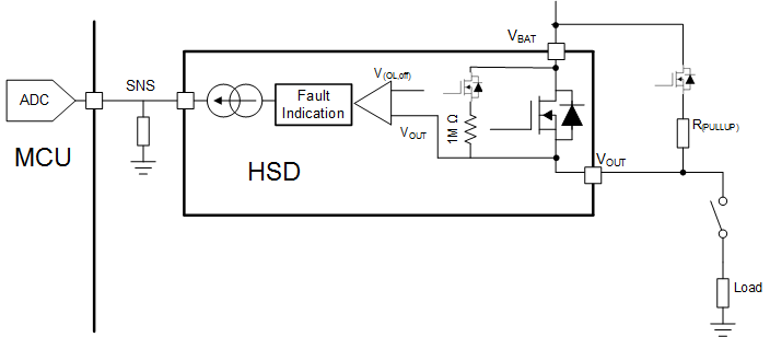
While the switch is disabled, if DIA_EN is high, an internal comparator will detect the condition of VOUT. If the load is disconnected (open load condition) or there is a short to battery the VOUT voltage will be higher than the open load threshold (VOL,off) and a fault is indicated on the SNS pin and the FLT pin on version F. An internal pull-up of 1 MΩ is in series with an internal MOSFET switch, so no external component is required if a completely open load must be detected. However, if there is significant leakage or other current draw even when the load is disconnected, a lower value pull-up resistor and switch can be added externally to set the VOUT voltage above the VOL,off during open load conditions.
TPS1HB08-Q1 Open Load Detect.gif
This figure assumes that the device ground and the load ground are at the same potential. In a real system, there may be a ground shift voltage of 1 V to 2 V.
Figure 38. Short to Battery and Open Load Detection

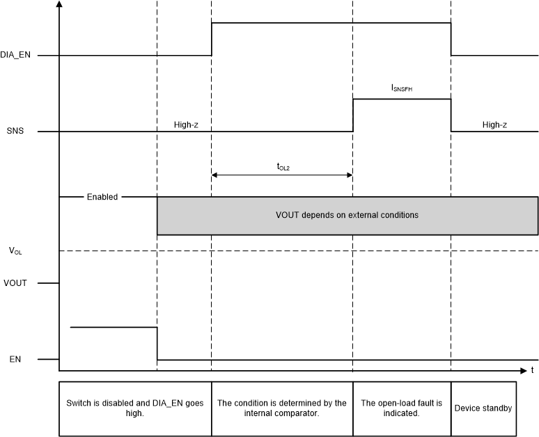
The detection circuitry is only enabled when DIA_EN = HIGH and EN = LOW. If VOUT > VOL, the SNS pin will go to the fault level, but if VOUT < VOL there will be no fault indication. The fault indication will only occur if the SEL1 pin is low.

While the switch is disabled and DIA_EN is high, the fault indication mechanisms will continuously represent the present status. For example, if VOUT decreases from greater than VOL to less than VOL, the fault indication is reset. Additionally, the fault indication is reset upon the falling edge of DIA_EN or the rising edge of EN.
TPS1HB08-Q1 timing-diagrams-td-08_TPS1HBxx.gifFigure 39. Open Load