JAJSHH4B may 2019 – february 2023 TPS1HB16-Q1
PRODUCTION DATA
- 1 特長
- 2 アプリケーション
- 3 概要
- 4 Revision History
- 5 Device Comparison Table
- 6 Pin Configuration and Functions
- 7 Specifications
- 8 Parameter Measurement Information
-
9 Detailed Description
- 9.1 Overview
- 9.2 Functional Block Diagram
- 9.3
Feature Description
- 9.3.1 Protection Mechanisms
- 9.3.2 Diagnostic Mechanisms
- 9.4 Device Functional Modes
- 10Application and Implementation
- 11Device and Documentation Support
- 12Mechanical, Packaging, and Orderable Information
パッケージ・オプション
メカニカル・データ(パッケージ|ピン)
- PWP|16
サーマルパッド・メカニカル・データ
- PWP|16
発注情報
10.2.3 Application Curves
When the device receives a rising edge on the EN pulse the output will turn on. After the turn-on delay time, the device VOUT goes to the VBB supply and begins outputting the steady state resistive current.
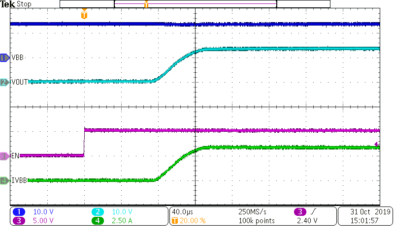 Figure 10-4 TPS1HB16-Q1 Turn-On Waveform (ROUT = 4 Ω)
When the device turns off on a falling edge of EN, the channel IOUT will go to zero and the VOUT will drop to zero as well as shown.
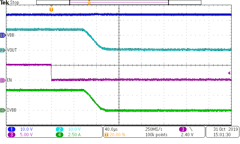 Figure 10-5 TPS1HB16-Q1 Turn-Off Waveform (ROUT = 4 Ω)
When there is a load step, the SNS current output will follow the load current with a slight delay. The image shows the output current temporarily increase from 1 A to 5 A and then return to 1 A. In this situation, the output current is accurately modeled throughout the pulse by the voltage on the SNS pin allowing for accurate diagnostics.
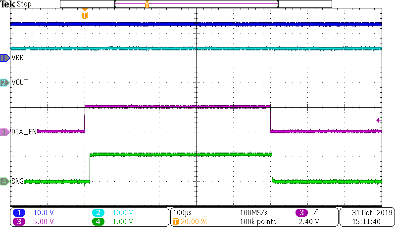 Figure 10-6 TPS1HB16-Q1 SNS Settling Time
If the device has a no-load case due to an open load or cable, the device will register the fault even in an off-state if the DIAG_EN pin is high. Figure 10-7 shows the device behavior when an open load event is registered with EN low and DIAG_EN is raised. Systems can PWM DIAG_EN to lower system power losses while still watching for open load events and the same timing applies.
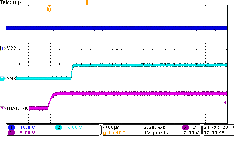 Figure 10-7 Open Load (tOL) Detection Time
If the output of the TPS1HB16-Q1 is short-circuited, the device will protect the system from failure. Depending on the device version and RILIM, the current limit set-point will vary. The waveforms below show examples of the current limit behavior when the device is enabled into a short circuit with a test setup according to AEC-Q100-012. In each case, the RILIM pin has a 5 kΩ resistor to set the current limit.
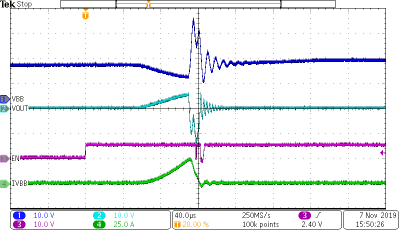 Figure 10-8 TPS1HB16-Q1 Version A Short Circuit Waveform
 Figure 10-9 TPS1HB16-Q1 Version B Short Circuit Waveform