SLVSA01C May 2011 – June 2016 TPS2062-Q1 , TPS2065-Q1
PRODUCTION DATA.
- 1 Features
- 2 Applications
- 3 Description
- 4 Revision History
- 5 Pin Configuration and Functions
- 6 Specifications
- 7 Parameter Measurement Information
- 8 Detailed Description
-
9 Application and Implementation
- 9.1
Application Information
- 9.1.1 Overcurrent
- 9.1.2 OC Response
- 9.1.3 Undervoltage Lockout (UVLO)
- 9.1.4 Universal Serial Bus (USB) Applications
- 9.1.5 Host, Self-Powered (SPH), and Bus-Powered Hubs (BPH)
- 9.1.6 Low-Power Bus-Powered and High-Power Bus-Powered Functions
- 9.1.7 USB Power-Distribution Requirements
- 9.1.8 Generic Hot-Plug Applications
- 9.2 Typical Application
- 9.1
Application Information
- 10Power Supply Recommendations
- 11Layout
- 12Device and Documentation Support
- 13Mechanical, Packaging, and Orderable Information
パッケージ・オプション
メカニカル・データ(パッケージ|ピン)
- DGN|8
サーマルパッド・メカニカル・データ
- DGN|8
発注情報
6 Specifications
6.1 Absolute Maximum Ratings
over operating free-air temperature range unless otherwise noted(1)| MIN | MAX | UNIT | |
|---|---|---|---|
| Input voltage, VI(IN)(2) | –0.3 | 6 | V |
| Output voltage(2), VO(OUTx) | –0.3 | 6 | V |
| Input voltage, VI(ENx) | –0.3 | 6 | V |
| Voltage, VI(OCx) | –0.3 | 6 | V |
| Continuous output current, IO(OUTx) | Internally limited | ||
| Continuous total power dissipation | See Dissipation Ratings | ||
| Operating virtual junction temperature range, TJ | –40 | 150 | °C |
| Storage temperature range, Tstg | –65 | 150 | °C |
(1) Stresses beyond those listed under Absolute Maximum Ratings may cause permanent damage to the device. These are stress ratings only, which do not imply functional operation of the device at these or any other conditions beyond those indicated under Recommended Operating Conditions. Exposure to absolute-maximum-rated conditions for extended periods may affect device reliability.
(2) All voltages are with respect to GND.
6.2 ESD Ratings
| VALUE | UNIT | |||
|---|---|---|---|---|
| V(ESD) | Electrostatic discharge | Human-body model (HBM), per AEC Q100-002(1) | ±2000 | V |
| Charged-device model (CDM), per AEC Q100-011 | ±1000 | |||
| Machine model (MM) | ±100 | |||
(1) AEC Q100-002 indicates that HBM stressing shall be in accordance with the ANSI/ESDA/JEDEC JS-001 specification.
6.3 Recommended Operating Conditions
| MIN | MAX | UNIT | |
|---|---|---|---|
| Input voltage, VI(IN) | 2.7 | 5.5 | V |
| Input voltage, VI(ENx) | 0 | 5.5 | V |
| Continuous output current, IO(OUTx) | 0 | 1 | A |
| Ambient temperature, TA | –40 | 125 | °C |
| Operating virtual junction temperature, TJ | –40 | 150 | °C |
6.4 Thermal Information
| THERMAL METRIC(1) | TPS2062-Q1 | TPS2065-Q1 | UNIT | |
|---|---|---|---|---|
| DGN (MSOP-PowerPAD) |
DGN (MSOP-PowerPAD) |
|||
| 8 PINS | 8 PINS | |||
| RθJA | Junction-to-ambient thermal resistance | 65 | 57.3 | °C/W |
| RθJC(top) | Junction-to-case (top) thermal resistance | 52.8 | 54.7 | °C/W |
| RθJB | Junction-to-board thermal resistance | 42.3 | 38.8 | °C/W |
| ψJT | Junction-to-top characterization parameter | 3.1 | 3.9 | °C/W |
| ψJB | Junction-to-board characterization parameter | 41.9 | 38.6 | °C/W |
| RθJC(bot) | Junction-to-case (bottom) thermal resistance | 17.7 | 10.1 | °C/W |
(1) For more information about traditional and new thermal metrics, see the Semiconductor and IC Package Thermal Metrics application report.
6.5 Electrical Characteristics
over recommended operating junction temperature range, VI(IN) = 5.5 V, IO = 1 A, VI(ENx) = 0 V for TPS2062-Q1 or VI(EN) = 5.5 V for TPS2065-Q1 (unless otherwise noted)| PARAMETER | TEST CONDITIONS(1) | MIN | TYP | MAX | UNIT | ||
|---|---|---|---|---|---|---|---|
| POWER SWITCH | |||||||
| rDS(ON) | Static drain-source ON-state resistance, 5-V operation and 3.3-V operation | VI(IN) = 5 V or 3.3 V, IO = 1 A, –40°C ≤ TA ≤ 125°C | 70 | 135 | mΩ | ||
| Static drain-source ON-state resistance, 2.7-V operation(2) | VI(IN) = 2.7 V, IO = 1 A, –40°C ≤ TA ≤ 125°C | 75 | 150 | mΩ | |||
| tr | Rise time, output | CL = 1 μF, RL= 5 Ω, TA = 25°C | VI(IN) = 5.5 V | 0.6 | 1.5 | ms | |
| VI(IN) = 2.7 V | 0.4 | 1 | |||||
| tf | Fall time, output | CL = 1 μF, RL= 5 Ω, TA = 25°C | VI(IN) = 5.5 V | 0.05 | 0.5 | ms | |
| VI(IN) = 2.7 V | 0.05 | 0.5 | |||||
| ENABLE INPUT EN OR EN | |||||||
| VIH | High-level input voltage | 2.7 V ≤ VI(IN) ≤ 5.5 V | 2 | V | |||
| VIL | Low-level input voltage | 2.7 V ≤ VI(IN) ≤ 5.5 V | 0.8 | ||||
| II | Input current | VI(ENx) = 0 V or 5.5 V | –1 | 1 | μA | ||
| tON | Turnon time | CL = 100 μF, RL= 5 Ω | 3 | ms | |||
| toff | Turnoff time | CL = 100 μF, RL= 5 Ω | 10 | ||||
| CURRENT LIMIT | |||||||
| IOS | Short-circuit output current(1) | VI(IN) = 5 V, OUT connected to GND, Device enabled into short-circuit |
TA = 25°C | 1.1 | 1.5 | 1.9 | A |
| –40°C ≤ TA ≤ 125°C | 1.1 | 1.5 | 2.1 | ||||
| IOC_TRIP | Overcurrent trip threshold | VI(IN) = 5 V, current ramp (≤ 100 A/s) on OUT | 1.6 | 2.3 | 2.9 | A | |
| SUPPLY CURRENT (TPS2062-Q1) | |||||||
| Supply current, low-level output | No load on OUT, VI(ENx) = 5.5 V | TA = 25°C | 0.5 | 1 | μA | ||
| –40°C ≤ TA ≤ 125°C | 0.5 | 5 | |||||
| Supply current, high-level output | No load on OUT, VI(ENx) = 0 V | TA = 25°C | 50 | 70 | μA | ||
| –40°C ≤ TA ≤ 125°C | 50 | 90 | |||||
| Leakage current | OUT connected to ground, VI(ENx) = 5.5 V | –40°C ≤ TA ≤ 125°C | 1 | μA | |||
| Reverse leakage current | VI(OUTx) = 5.5 V, IN = ground | TA = 25°C | 0.2 | μA | |||
| SUPPLY CURRENT (TPS2065-Q1) | |||||||
| Supply current, low-level output | No load on OUT, VI(EN) = 0 V | TA = 25°C | 0.5 | 1 | μA | ||
| –40°C ≤ TA ≤ 125°C | 0.5 | 5 | |||||
| Supply current, high-level output | No load on OUT, VI(EN) = 5.5 V | TA = 25°C | 43 | 60 | μA | ||
| –40°C ≤ TA ≤ 125°C | 43 | 70 | |||||
| Leakage current | OUT connected to ground, VI(EN) = 0 V | –40°C ≤ TA ≤ 125°C | 1 | μA | |||
| Reverse leakage current | VI(OUTx) = 5.5 V, IN = ground | TA = 25°C | 0 | μA | |||
| UNDERVOLTAGE LOCKOUT | |||||||
| Low-level input voltage, IN | 2 | 2.5 | V | ||||
| Hysteresis, IN | TA = 25°C | 75 | mV | ||||
| OVERCURRENT OC1 AND OC2 | |||||||
| Output low voltage, VOL(OCx) | IO(OCx) = 5 mA | 0.4 | V | ||||
| Off-state current | VO(OCx) = 5 V or 3.3 V | 1 | μA | ||||
| OC deglitch(2) | OCx assertion or deassertion | 4 | 8 | 15 | ms | ||
| THERMAL SHUTDOWN(3) | |||||||
| Thermal shutdown threshold | 135 | °C | |||||
| Recovery from thermal shutdown | 125 | °C | |||||
| Hysteresis | 10 | °C | |||||
(1) Pulse-testing techniques maintain junction temperature close to ambient temperature; thermal effects must be taken into account separately.
(2) Not tested in production, specified by design.
(3) The thermal shutdown only reacts under overcurrent conditions.
6.6 Dissipation Ratings
| PACKAGE | TA ≤ 25°C POWER RATING |
DERATING FACTOR ABOVE TA = 25°C |
TA = 125°C POWER RATING |
|---|---|---|---|
| DGN-8 | 2.14 W | 17.123 mW/°C | 428 mW |
6.7 Typical Characteristics
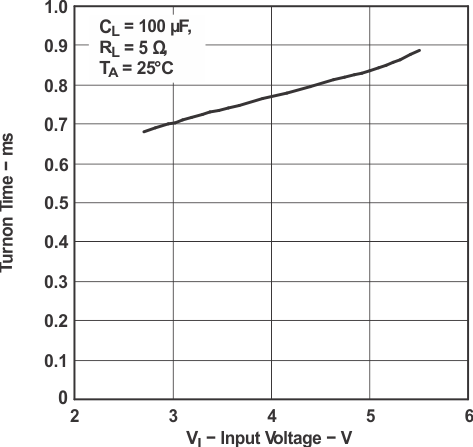

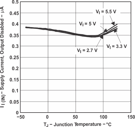
vs Junction Temperature

vs Junction Temperature
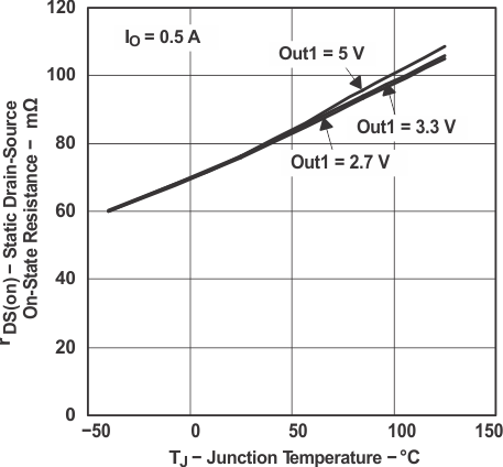
vs Junction Temperature


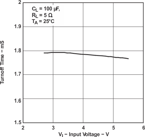


vs Junction Temperature

vs Junction Temperature
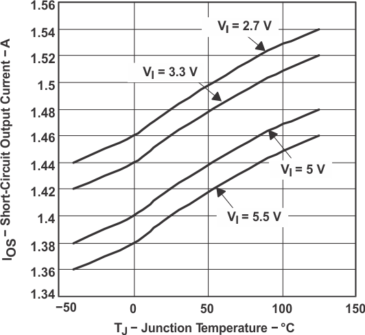
vs Junction Temperature
