JAJSCP4 December 2016 TPS2065D
PRODUCTION DATA.
9 Application and Implementation
NOTE
Information in the following applications sections is not part of the TI component specification, and TI does not warrant its accuracy or completeness. TI’s customers are responsible for determining suitability of components for their purposes. Customers should validate and test their design implementation to confirm system functionality.
9.1 Application Information
The TPS2065D current limited power switch uses N-channel MOSFETs in applications requiring continuous load current. The device enters constant-current mode when the load exceeds the current limit threshold.
9.2 Typical Application
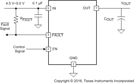 Figure 22. Typical Application Schematic
9.2.1 Design Requirements
For this design example, use the following input parameters:
- The TPS2065D operates from a 5 V±0.5V rail.
- What is the normal operation current, for example, the maximum allowable current drawn by portable equipment for USB 3.0 port is 900 mA, so the normal operation current is 900 mA, and the minimum current limit of power switch must exceed 900 mA to avoid false trigger during normal operation. For the TPS2065D device, target 1 A continuous output current application.
- What is the maximum allowable current provided by up-stream power, the maximum current limit of power switch that must lower it to ensure power switch can protect the up-stream power when overload is encountered at the output of power switch. For the TPS2065D device, the maximum IOS is 1.8 A.
9.2.2 Detailed Design Procedure
To begin the design process a few parameters must be decided upon. The designer needs to know the following:
- Normal input operation voltage
- Output continuous current
- Maximum up-stream power supply output current
9.2.2.1 Input and Output Capacitance
Input and output capacitance improves the performance of the device; the actual capacitance should be optimized for the particular application. For all applications, TI recommends placing a 0.1-µF or greater ceramic bypass capacitor between IN and GND, as close to the device as possible for local noise decoupling.
All protection circuits such as the TPS2065D has the potential for input voltage overshoots and output voltage undershoots.
Input voltage overshoots can be caused by either of two effects. The first cause is an abrupt application of input voltage in conjunction with input power bus inductance and input capacitance when the IN terminal is high impedance (before turnon). Theoretically, the peak voltage is 2× the applied. The second cause is due to the abrupt reduction of output short circuit current when the device turns off and energy stored in the input inductance drives the input voltage high. Input voltage droops may also occur with large load steps and as the device output is shorted. Applications with large input inductance (for example, connecting the evaluation board to the bench power-supply through long cables) may require large input capacitance reduce the voltage overshoot from exceeding the absolute maximum voltage of the device. The fast current limit speed of the device to hard output short circuits isolates the input bus from faults. However, ceramic input capacitance in the range of 1 µF to 22 µF adjacent to the device input aids in both speeding the response time and limiting the transient seen on the input power bus. Momentary input transients to 6.5 V are permitted.
Output voltage undershoot is caused by the inductance of the output power bus just after a short has occurred and the TPS2065D has abruptly reduced OUT current. Energy stored in the inductance drives the OUT voltage down and potentially negative as it discharges. Applications with large output inductance (such as from a cable) benefit from use of a high-value output capacitor to control the voltage undershoot. When implementing USB standard applications, a 120 µF minimum output capacitance is required. Typically a 150-µF electrolytic capacitor is used, which is sufficient to control voltage undershoots. However, if the application does not require 120 µF of capacitance, and there is potential to drive the output negative, then TI recommends a minimum of 10-µF ceramic capacitance on the output. The voltage undershoot should be controlled to less than 1.5 V for 10 µs.
9.2.3 Application Curves
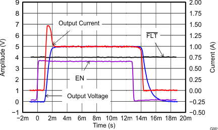
| VIN = 5 V | COUT = 150 µF | RLOAD = 5 mΩ |
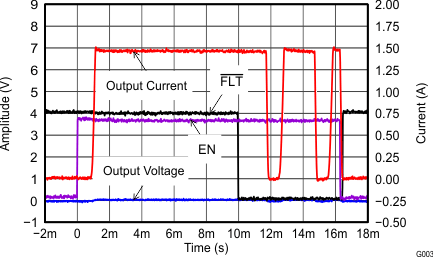
| VIN = 5 V | COUT = 150 µF | RLOAD = 0 Ω |
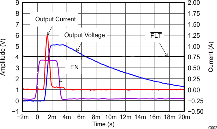
| VIN = 5 V | COUT = 150 µF | RLOAD = 100 Ω |

| VIN = 5 V | COUT = 150 µF | RLOAD = 50 mΩ |
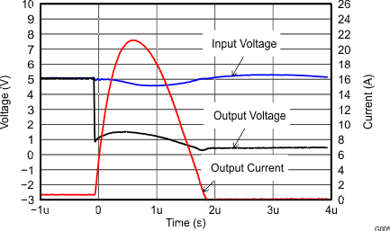
| VIN = 5 V | COUT = 150 µF |
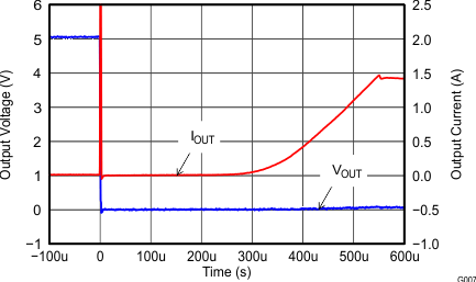
| VIN = 5 V | COUT = 0 µF | RLOAD = 50 mΩ |
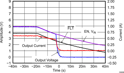
| VIN = 5 V | COUT = 150 µF | RLOAD = 7.5 Ω |
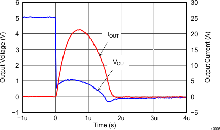
| VIN = 5 V | COUT = 0 µF | RLOAD = 50 mΩ |
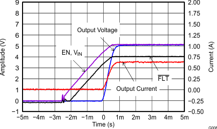
| VIN = 5 V | COUT = 150 µF | RLOAD = 7.5 mΩ |