JAJSPX3B February 2007 – June 2024 TPS2062-1 , TPS2065-1 , TPS2066-1
PRODUCTION DATA
- 1
- 1 特長
- 2 アプリケーション
- 3 概要
- 4 Pin Configuration and Functions
- 5 Specifications
- 6 Parameter Measurement Information
- 7 Detailed Description
-
8 Application and Implementation
- 8.1
Application Information
- 8.1.1 Power-Supply Considerations
- 8.1.2 OC Response
- 8.1.3 Power Dissipation and Junction Temperature
- 8.1.4 Thermal Protection
- 8.1.5 Undervoltage Lockout (UVLO)
- 8.1.6 Universal Serial Bus (USB) Applications
- 8.1.7 Host/Self-Powered and Bus-Powered Hubs
- 8.1.8 Low-Power Bus-Powered and High-Power Bus-Powered Functions
- 8.1.9 USB Power-Distribution Requirements
- 8.1.10 Generic Hot-Plug Applications
- 8.1
Application Information
- 9 Device and Documentation Support
- 10Revision History
- 11Mechanical, Packaging, and Orderable Information
パッケージ・オプション
デバイスごとのパッケージ図は、PDF版データシートをご参照ください。
メカニカル・データ(パッケージ|ピン)
- DGN|8
サーマルパッド・メカニカル・データ
- DGN|8
発注情報
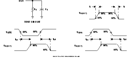 Figure 6-1 Test Circuit and Voltage Waveforms
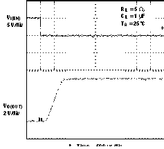 Figure 6-2 Turnon Delay and Rise Time With 1-µF Load
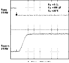 Figure 6-4 Turnon Delay and Rise Time With 100-µF Load
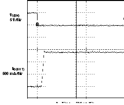 Figure 6-6 Short-Circuit Current, Device Enabled Into Short
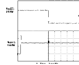 Figure 6-8 2-Ω
Load Connected to Enabled Device
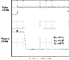 Figure 6-3 Turnoff Delay and Fall Time With 1-µF Load
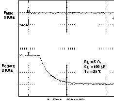 Figure 6-5 Turnoff Delay and Fall Time With 100-µF Load
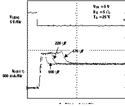 Figure 6-7 Inrush Current With Different Load Capacitance
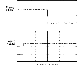 Figure 6-9 1-Ω
Load Connected to Enabled Device