JAJSCS0C December 2016 – January 2018 TPS22810
PRODUCTION DATA.
- 1 特長
- 2 アプリケーション
- 3 概要
- 4 改訂履歴
- 5 Device Comparison Table
- 6 Pin Configuration and Functions
- 7 Specifications
- 8 Parameter Measurement Information
- 9 Detailed Description
- 10Application and Implementation
- 11Power Supply Recommendations
- 12Layout
- 13デバイスおよびドキュメントのサポート
- 14メカニカル、パッケージ、および注文情報
パッケージ・オプション
メカニカル・データ(パッケージ|ピン)
サーマルパッド・メカニカル・データ
- DRV|6
発注情報
9.3.3 EN/UVLO
As an input pin, EN/UVLO controls the ON and OFF state of the internal MOSFET. In its high state, the internal MOSFET is enabled. A low on this pin turns off the internal MOSFET. High and Low levels are specified in the parametric table of the datasheet
A voltage V(EN/UVLO < V(ENF) on this pin turns off the internal FET, thus disconnecting VIN from VOUT, while voltage below V(SHUTF) takes the device into shutdown mode, with IQ less than 1 μA to ensure minimal power loss.
The EN/UVLO pin can be directly driven by a 1.8 V, 3.3 V or 5 V general purpose output pin.
The internal de-glitch delay on EN/UVLO falling edge is intentionally kept low (2.5 μs typical) for quick detection of power failure. For applications where a higher de-glitch delay on EN/UVLO is desired, or when the supply is particularly noisy, it is recommended to use an external bypass capacitor from EN/UVLO to GND.
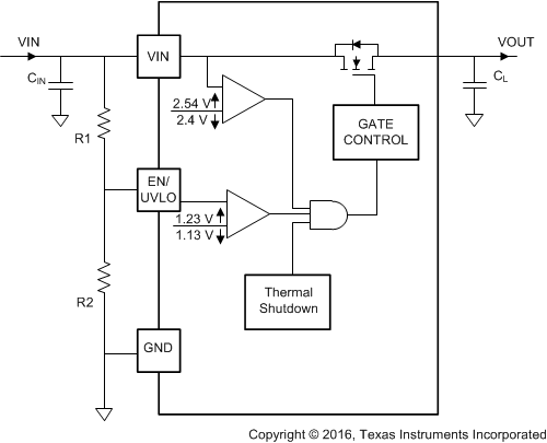
The undervoltage lock out can be programmed by using an external resistor divider from supply VIN terminal to EN/UVLO terminal to GND as shown in Figure 18. When an undervoltage or input power fail event is detected, the internal FET is quickly turned off. If the Under-Voltage Lock-Out function is not needed, the EN/UVLO terminal must be connected to the VIN terminal. EN/UVLO terminal must not be left floating.
The device also implements internal undervoltage-lockout (UVLO) circuitry on the VIN terminal. The device disables when the VIN terminal voltage falls below internal UVLO Threshold V(UVF). The internal UVLO threshold has a hysteresis of 125 mV (5% of V(UVR)). See Figure 19 and Figure 20.
 Figure 18. Configuring UVLO with External Resistor Network
 Figure 19. Using 1.8 V/3.3 V GPIO Signal Directly from Processor
 Figure 20. Default UVLO Threshold V(UVR) Using No Additional External Components