SLVSB34A October 2011 – June 2015 TPS22933
PRODUCTION DATA.
- 1 Features
- 2 Applications
- 3 Description
- 4 Revision History
- 5 Pin Configuration and Functions
- 6 Specifications
- 7 Parametric Measurement Information
- 8 Detailed Description
- 9 Application and Implementation
- 10Power Supply Recommendations
- 11Layout
- 12Device and Documentation Support
- 13Mechanical, Packaging, and Orderable Information
1 Features
- Three Integrated Load Switches Automatically Choose Highest Input
- Integrated 3.6-V Fixed LDO
- Switched and Always on LDO Outputs
- µQFN package 1.5 mm × 1.5 mm
- Input Voltage Range: 2.5 V to 12 V
- Low ON-Resistance (rON)
- rON = 2.4 Ω at VIN = 5.0 V
- rON = 2.6 Ω at VIN = 4.2 V
- 50-mA Maximum Continuous Current
- Low Threshold Control Input (EN)
- Switchover Time of 18 µs (typical)
2 Applications
- Smart Phones
- GPS Devices
- Digital Cameras
- Portable Industrial Equipment
- Portable Medical Equipment
- Portable Media Players
- Portable Instrumentation
3 Description
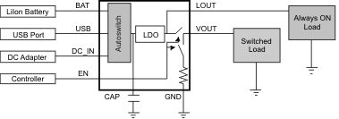
The TPS22933 device is a small, low rON, triple-input power multiplexer with auto-input selection and a low-dropout linear regulator. The device contains three P-channel MOSFETs that can operate over an input voltage range of 2.5 V to 12 V. The TPS22933 automatically selects the highest level (from BAT, USB, and DC_IN) and enables that input to source the LDO. LOUT is an always-on output from the LDO. The Enable function (EN pin) allows VOUT to be switched on or off, enables a quick discharge resistor, and is capable of interfacing directly with low-voltage control signals.
The TPS22933 is available in a small, space-saving 8-pin µQFN package and is characterized for operation over the free-air temperature range of –40ºC to 85ºC.
Device Information(1)
| PART NUMBER | PACKAGE | BODY SIZE (NOM) |
|---|---|---|
| TPS22933 | UQFN (8) | 1.50 mm × 1.50 mm |
- For all available packages, see the orderable addendum at the end of the data sheet.
Typical Application Diagram
