SLVS984B September 2009 – March 2015 TPS22946
PRODUCTION DATA.
- 1 Features
- 2 Applications
- 3 Description
- 4 Revision History
- 5 Pin Configuration and Functions
- 6 Specifications
- 7 Parameter Measurement Information
- 8 Detailed Description
- 9 Application and Implementation
- 10Power Supply Recommendations
- 11Layout
- 12Device and Documentation Support
- 13Mechanical, Packaging, and Orderable Information
1 Features
- Ultralow Quiescent Current 1 μA (Typical)
at VIN = 1.8 V - Input Voltage Range: 1.62 V to 5.5 V
- Low ON-Resistance
- rON = 300 mΩ at VIN = 5.5 V
- rON = 400 mΩ at VIN = 3.3 V
- rON = 500 mΩ at VIN = 2.5 V
- rON = 600 mΩ at VIN = 1.8 V
- Selectable Minimum Current Limit:
155 mA, 70 mA, or 30 mA - Integrated Inrush Current Time-out (8 ms)
- Shutdown Current: < 1 μA
- Thermal Shutdown
- Fault Blanking
- Auto Restart
- Overcurrent Condition Time-out (Automatic Disable for Permanent Overcurrent)
- 1.8-V Compatible Control Input
- ESD Performance Tested Per JESD 22
- 6000-V Human-Body Model
(A114-B, Class II)
- 6000-V Human-Body Model
- Tiny DSGBA Package 1.4 mm × 0.9 mm (YZP)
2 Applications
- Fingerprint Module Protection
- Portable Consumer Electronics
- Mobile Phones
- Smartphones
- Notebooks
- GPS Devices
3 Description
The TPS22946 is an ultralow power load switch that provides protection to systems and loads in high-current conditions. The device contains a 300-mΩ current-limited P-channel MOSFET that can operate over an input voltage range of 1.62 V to 5.5 V. The switch is controlled by an on/off input (ON), which can interface directly with low-voltage control signals. The TPS22946 includes thermal shutdown protection that prevents damage to the device when a continuous over-current condition causes excessive heating by turning off the switch.
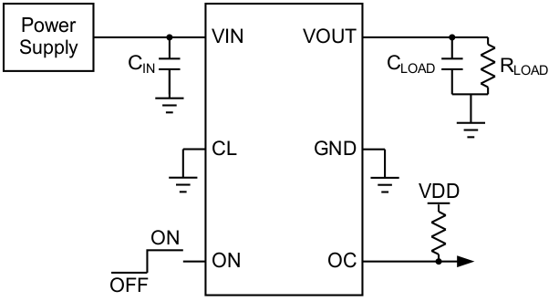
When the switch current reaches the maximum limit, the TPS22946 operates in a constant-current mode to prohibit excessive currents from causing damage. The current limit can be selected using the CL input: a high CL input sets the current limit to 155 mA, a low CL input sets the current limit to 70 mA, and a floating CL input sets the current limit to 30 mA.
If the constant current condition persists after 10 ms, the switch is turned off and the fault signal pin (OC) is pulled low. The TPS22946 has an auto-restart feature which turns the switch on again after 70 ms if the ON pin is still active. If the TPS22946 remains in an over-current condition for 5 seconds, the device shuts off until it is turned on again by setting the ON control signal off and then on.
If the device is used to protect an LDO, the inrush current required by the LDO at startup can, in some cases, exceed the current limit and initiate a blanking (current limiting) condition. The TPS22946 provides allowance for this scenario during startup of the LDO by temporarily increasing the current limit to 435 mA for 8 ms after the load switch is enabled.
The TPS22946 is available in space-saving 6-pin DSBGA (YZP) package. The device is characterized for operation over the free-air temperature range of –40°C to 85°C.
Device Information(1)
| PART NUMBER | PACKAGE | BODY SIZE (NOM) |
|---|---|---|
| TPS22946 | DSBGA (6) | 0.90 mm × 1.40 mm |
- For all available packages, see the orderable addendum at the end of the data sheet.
Typical Application Schematic
