SLVS908D February 2009 – June 2015 TPS22949
PRODUCTION DATA.
- 1 Features
- 2 Applications
- 3 Description
- 4 Revision History
- 5 Description (continued)
- 6 Pin Configuration and Functions
-
7 Specifications
- 7.1 Absolute Maximum Ratings
- 7.2 ESD Ratings
- 7.3 Recommended Operating Conditions
- 7.4 Thermal Information
- 7.5 Electrical Characteristics
- 7.6 Current Limiter Electrical Characteristics
- 7.7 Low-Noise LDO Regulator Electrical Characteristics
- 7.8 Current Limiter Switching Characteristics
- 7.9 Typical Characteristics
- 8 Detailed Description
- 9 Application and Implementation
- 10Power Supply Recommendations
- 11Layout
- 12Device and Documentation Support
- 13Mechanical, Packaging, and Orderable Information
パッケージ・オプション
メカニカル・データ(パッケージ|ピン)
- DRG|8
サーマルパッド・メカニカル・データ
- DRG|8
発注情報
9 Application and Implementation
NOTE
Information in the following applications sections is not part of the TI component specification, and TI does not warrant its accuracy or completeness. TI’s customers are responsible for determining suitability of components for their purposes. Customers should validate and test their design implementation to confirm system functionality.
9.1 Application Information
This application illustrates the TPS22949 and TPS22949A configured with a 100-mA sinking load with both enables tied to the same input voltage.
9.1.1 Input Voltage
The input voltage (VIN) of the current limiter is set from 1.62 V to 4.5 V, however if both the current limiter and the LDO are enabled, the user must be careful to keep the input voltage (VIN) greater than 1.8 V + (voltage drop through the switch) + (voltage drop through the LDO); otherwise, the LDO does not have a high enough internal input signal to operate properly.
A current limiter input voltage ramp time less than the blanking time (approximately 10 ms typical) is recommended. If the ramp time extends beyond the blanking period, then the current limiter goes into recycle, and the system may not start or operate properly.
9.1.2 Input/Output Capacitors
Although an input capacitor is not required for stability of on the input pin (VIN), it is good analog design practice to connect a 0.1-μF to 1-μF low equivalent series resistance (ESR) capacitor across the IN pin input supply near the regulator. This capacitor counteracts reactive input sources and improves transient response, noise rejection, and ripple rejection. A higher value capacitor may be necessary if large, fast rise time load transients are anticipated, or if the device is located close to the power source. If source impedance is not sufficiently low, a 0.1-μF input capacitor may be necessary to ensure stability. The V+ bias pin does not require an input capacitor because it does not source high currents. However, if source impedance is not sufficiently low, a small 0.1-μF bypass capacitor is recommended.
A 0.1-μF capacitor CCL, must be placed between VOUTCL and GND. This capacitor prevents parasitic board inductances from forcing VOUTCL below GND when the switch turns off.
9.2 Typical Application
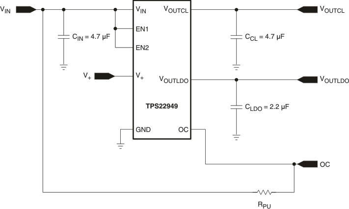
 Figure 43. TPS22949/TPS22949A Typical Application With Both Enable Pins Tied to the Input Voltage
9.2.1 Design Requirements
For this design example, use the parameters listed in Table 2 as the input parameters.
Table 2. Design Parameters
| DESIGN PARAMETER | EXAMPLE VALUE |
|---|---|
| VIN | 3.3 V |
| V+ | 3.3 V |
| CIN | 4.7 µF |
| CLDO | 2.2 µF |
9.2.2 Detailed Design Procedure
9.2.2.1 Start-Up Sequence
For the TPS22949, the total output capacitance must be kept below a maximum value, CCL(max), to prevent the part from registering an overcurrent condition and turning off the switch. The maximum output capacitance can be determined from Equation 1:
Due to the integral body diode in the PMOS switch, a CIN greater than CCL is highly recommended. A CCL greater than CIN can cause VOUTCL to exceed VIN when the system supply is removed. This could result in current flow through the body diode from VOUTCL to VIN.
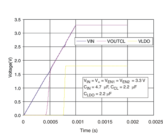
On TPS22949, a storage capacitor (CCL) at the output of the current limiter is recommended to provide enough current to the LDO during the start-up sequence. The storage capacitor is needed to reduce the amount of inrush current supplied through the current-limited load switch to the LDO during the power-up sequence (see Figure 44). If the CCL capacitor is too small, the inrush current needed to start the LDO and charge CLDO could be interpreted by the current limiter as an overcurrent and, therefore, trigger the current-limiting feature of the switch. The switch would then try to limit the current to the 100-mA limit, and the user would see an undesired drop on the supply line (see Figure 45).
On TPS22949A, the storage capacitor (CCL) is not required. TPS22949A integrates an additional internal circuitry that increases the current limit of the switch to approximately 750 mA (that is, ILIM(INRUSH)) for about 250 μs (that is, tINRUSH), initiated when the internal circuitry of the LDO is operating properly (that is, when the UVLO of the LDO bias (V+) is disabled (V+ > 2.6 V). Because the current limit is increased during the power-up sequence, a potential inrush current through the LDO is not interpreted by the current limiter as an overcurrent. The current needed by the LDO is then be supplied by the input capacitor (CIN) of the current limiter (see Figure 45).
The TPS22949 LDO (VOUTLDO) is designed to be stable with standard ceramic capacitors with values of 2.2 μF or larger at the output. X5R- and X7R-type capacitors are best because they have minimal variation in value and ESR over temperature. Maximum ESR must be less than 250 mΩ. Figure 43, Figure 44, and Figure 45 illustrate the behavior of the TPS22949 and TPS22949A with a 100-mA sinking load and different capacitor values for a typical application where both enables are tied to the same input voltage (see Figure 43).
9.2.3 Application Curves

 Figure 46. TPS22949A Power-Up Sequence
 Figure 45. TPS22949 Power-Up Sequence
9.3 System Examples
 Figure 47. TPS22949 Typical Application Schematic
 Figure 48. TPS22949A Typical Application Schematic