SLVS908D February 2009 – June 2015 TPS22949
PRODUCTION DATA.
- 1 Features
- 2 Applications
- 3 Description
- 4 Revision History
- 5 Description (continued)
- 6 Pin Configuration and Functions
-
7 Specifications
- 7.1 Absolute Maximum Ratings
- 7.2 ESD Ratings
- 7.3 Recommended Operating Conditions
- 7.4 Thermal Information
- 7.5 Electrical Characteristics
- 7.6 Current Limiter Electrical Characteristics
- 7.7 Low-Noise LDO Regulator Electrical Characteristics
- 7.8 Current Limiter Switching Characteristics
- 7.9 Typical Characteristics
- 8 Detailed Description
- 9 Application and Implementation
- 10Power Supply Recommendations
- 11Layout
- 12Device and Documentation Support
- 13Mechanical, Packaging, and Orderable Information
パッケージ・オプション
メカニカル・データ(パッケージ|ピン)
- DRG|8
サーマルパッド・メカニカル・データ
- DRG|8
発注情報
6 Pin Configuration and Functions
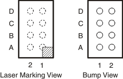
YZP Package
8-Pin DSBGA
Top View

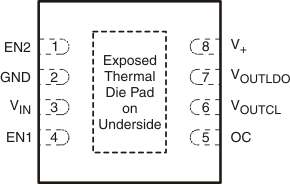
DRG Package
8-Pin WSON
Top View

The exposed center pad, if used, must be connected as a secondary GND or left electrically open.
Pin Functions
| PIN | I/O | DESCRIPTION | ||
|---|---|---|---|---|
| NAME | DSBGA | WSON | ||
| EN1 | D2 | 4 | I | Power switch control input. Active high. Do not leave floating. |
| EN2 | A2 | 1 | I | LDO control input. Active high. Do not leave floating. |
| GND | B2 | 2 | — | Ground |
| OC | D1 | 5 | O | Overcurrent output flag. Active low, open-drain output that indicates an overcurrent, supply undervoltage, or overtemperature state. |
| V+ | A1 | 8 | I | Supply voltage |
| VIN | C2 | 3 | I | Supply input. Input to the power switch; bypass this input with a ceramic capacitor to ground. |
| VOUTCL | C1 | 6 | O | Switch output. Output of the power switch |
| VOUTLDO | B1 | 7 | O | LDO output. Output of the RF LDO fixed to 1.8 V(1). |
(1) Output voltages from 0.9 V to 3.6 V in 50-mV increments are available through the use of innovative factory EEPROM programming; minimum order quantities may apply. Contact factory for details and availability.
YZP Package Pin Assignments
| D | EN1 | OC |
| C | VIN | VOUTCL |
| B | GND | VOUTLDO |
| A | EN2 | V+ |
| 2 | 1 |