SLVS788D February 2009 – November 2016 TPS22951
PRODUCTION DATA.
- 1 Features
- 2 Applications
- 3 Description
- 4 Revision History
- 5 Pin Configurations and Functions
- 6 Specifications
- 7 Parameter Measurement Information
- 8 Detailed Description
- 9 Application and Implementation
- 10Power Supply Recommendations
- 11Layout
- 12Device and Documentation Support
- 13Mechanical, Packaging, and Orderable Information
6 Specifications
6.1 Absolute Maximum Ratings
over operating free-air temperature range (unless otherwise noted) (1)| MIN | MAX | UNIT | |||
|---|---|---|---|---|---|
| VCC (2) | Supply voltage | –0.3 | 6 | V | |
| VO(PWR) (2) | Output voltage | –0.3 | VCC + 0.3 | V | |
| VI(EN), VI(DET) | Input voltage | –0.3 | 6 | V | |
| VO(PG) | Voltage | –0.3 | 6 | V | |
| IO(PWR) | Continuous output current | Internally limited | |||
| Continuous total power dissipation | See the Thermal Information section | ||||
| Lead temperature soldering 1,6 mm (1/16 in) from case for 10 s | –0.3 | 6 | V | ||
| TJ | Operating virtual junction temperature | –40 | 85 | °C | |
| Tstg | Storage temperature | –65 | 150 | °C | |
(1) Stresses beyond those listed under Absolute Maximum Ratings may cause permanent damage to the device. These are stress ratings only, which do not imply functional operation of the device at these or any other conditions beyond those indicated under Recommended Operating Conditions. Exposure to absolute-maximum-rated conditions for extended periods may affect device reliability.
(2) All voltages are with respect to GND.
6.2 ESD Ratings
| VALUE | UNIT | |||
|---|---|---|---|---|
| V(ESD) | Electrostatic discharge | Human body model (HBM), per ANSI/ESDA/JEDEC JS-001 (1) | 4000 | V |
| Charged-device model (CDM), per JEDEC specification JESD22-C101 (2) | 1000 | |||
| Machine model (MM) | 400 | |||
(1) JEDEC document JEP155 states that 500-V HBM allows safe manufacturing with a standard ESD control process.
(2) JEDEC document JEP157 states that 250-V CDM allows safe manufacturing with a standard ESD control process.
6.3 Recommended Operating Conditions
| MIN | MAX | UNIT | ||
|---|---|---|---|---|
| VCC | Supply voltage | 2.2 | 5.3 | V |
| VI(EN), VI(DET) | Input voltage | 0 | VCC | V |
| IO(PWR) | Continuous output current | 0 | –600 | mA |
| TJ | Operating virtual junction temperature | –40 | 85 | °C |
6.4 Thermal Information
| THERMAL METRIC (1) | TPS22951 | UNIT | |
|---|---|---|---|
| YFP (DSBGA) | |||
| 6 PINS | |||
| RθJA | Junction-to-ambient thermal resistance | 125.1 | °C/W |
| RθJC(top) | Junction-to-case (top) thermal resistance | 1.4 | °C/W |
| RθJB | Junction-to-board thermal resistance | 26 | °C/W |
| ψJT | Junction-to-top characterization parameter | 0.3 | °C/W |
| ψJB | Junction-to-board characterization parameter | 26 | °C/W |
| RθJC(bot) | Junction-to-case (bottom) thermal resistance | N/A | °C/W |
(1) For more information about traditional and new thermal metrics, see the Semiconductor and IC Package Thermal Metrics application report.
6.5 Electrical Characteristics
over operating –40°C ≤ TJ ≤ +85°C range (unless otherwise noted)| PARAMETER | TEST CONDITIONS (1) | MIN | TYP | MAX | UNIT | |||
|---|---|---|---|---|---|---|---|---|
| POWER SWITCH | ||||||||
| rDS(on) | Static drain-source ON-state resistance, 3-V operation | VCC = 3 V, IO = 0.3 A | 1 | Ω | ||||
| Leakage current | PWR connected to GND, VI(EN) = 0 V | 1 | μA | |||||
| EN AND DET | ||||||||
| VIH | High-level input voltage | 2.8 V ≤ VCC ≤ 5.3 V | 1.35 | V | ||||
| VIL | Low-level input voltage | 2.8 V ≤ VCC ≤ 5.3 V | 0.45 | V | ||||
| II | Input current | VI(EN) or VI(DET) = 0 V or 5.3 V | 1 | μA | ||||
| CURRENT LIMIT | ||||||||
| IOS | Short-circuit output current | VCC = 2.8 V or 5.3 V, PWR connected to GND, Device enabled into short circuit |
–0.3 | –0.6 | A | |||
| SUPPLY CURRENT | ||||||||
| Supply current, enabled | No load on PWR, VCC = 5.3 V, VI(EN) = VCC, VI(DET) = VCC or 0 V |
100 | μA | |||||
| Supply current, disabled | No load on PWR, VCC = 5.3 V, VI(EN) = 0 V, VI(DET) = VCC or 0 V |
10 | μA | |||||
| PG | ||||||||
| VOL(PG) | Power Good output low voltage | I(PG) = 1 mA | 0.4 | V | ||||
| OFF-state current | V(PG) = 5.3 V | 1 | μA | |||||
| THERMAL SHUTDOWN | ||||||||
| Thermal shutdown threshold (2) | 135 | °C | ||||||
| Recovery from thermal shutdown (2) | 125 | °C | ||||||
| Hysteresis (2) | 25 | °C | ||||||
(1) Pulse-testing techniques maintain junction temperature close to ambient temperature; thermal effects must be taken into account separately.
(2) Not tested in production, specified by design
6.6 Timing Requirements
over operating free-air temperature range (unless otherwise noted)| MIN | MAX | UNIT | ||
|---|---|---|---|---|
| tsu | Setup time, DET low before EN high | 2 | μs | |
6.7 Switching Characteristics
over operating free-air temperature range (unless otherwise noted)| PARAMETER | TEST CONDITIONS | MIN | TYP | MAX | UNIT | |||
|---|---|---|---|---|---|---|---|---|
| POWER SWITCH | ||||||||
| tr (2) | Rise time, output | VCC = 5.3 V | CL = 1 μF, RL = 20 Ω |
TJ = 25°C | 41 | μs | ||
| VCC = 2.8 V | 6 | |||||||
| tf (2) | Fall time, output | VCC = 5.3 V | CL = 1 μF, RL = 20 Ω |
TJ = 25°C | 43 | μs | ||
| VCC = 2.8 V | 43 | |||||||
| EN AND DET | ||||||||
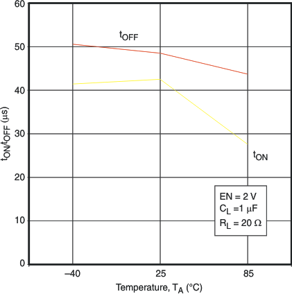
| ton (2) | Turnon time (EN to PWR) | VCC = 5.3 V | CL = 1 μF, RL = 20 Ω | 42 | μs | |||
| Turnon time (EN to PG) | CP = 15 pF, RP = 10 kΩ | 9.5 | ||||||
| toff (2) | Turnoff time (EN to PWR) | VCC = 5.3 V | CL = 1 μF, RL = 20 Ω | 48 | μs | |||
| Turnoff time (EN to PG) | CP = 15 pF, RP = 10 kΩ | 47 | ||||||
6.8 Typical Characteristics
 Figure 1. ON-State Resistance vs VCC
 Figure 3. ICC vs VCC, EN = GND
 Figure 5. tON/tOFF vs Temperature, VCC = 5.3 V
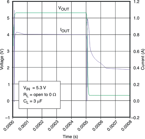
 Figure 7. Full-Load to Short-Circuit Transient Response
 Figure 9. No-Load to Short-Circuit Transient Response
 Figure 2. ICC vs VCC, EN = VCC
 Figure 4. trise/tfall vs Temperature, VCC = 5.3 V
 Figure 6. Device Enabled into Short-Circuit
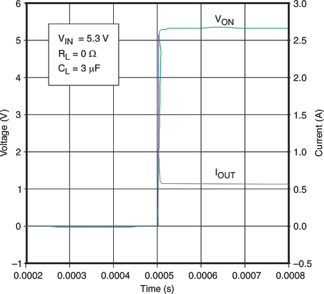
 Figure 8. Short-Circuit to Full-Load Recovery Response