JAJSF19A September   2017  – December 2017 TPS23521

PRODUCTION DATA.  

  1. 特長
  2. アプリケーション
  3. 概要
    1.     Device Images
      1.      概略回路図
  4. 改訂履歴
  5. Pin Configuration and Functions
    1.     Pin Functions
  6. Specifications
    1. 6.1 Absolute Maximum Ratings
    2. 6.2 ESD Ratings
    3. 6.3 Recommended Operating Conditions
    4. 6.4 Thermal Information
    5. 6.5 Electrical Characteristics
    6. 6.6 Switching Characteristics
    7. 6.7 Typical Characteristics
  7. Parameter Measurement Information
    1. 7.1 Relationship between Sense Voltage, Gate Current, and Timer
  8. Detailed Description
    1. 8.1 Overview
    2. 8.2 Functional Block Diagram
    3. 8.3 Feature Description
      1. 8.3.1 Current Limit
        1. 8.3.1.1 Programming the CL Switch-Over Threshold
        2. 8.3.1.2 Setting Up the PROG Pin
        3. 8.3.1.3 Programming CL1
        4. 8.3.1.4 Programming CL2
      2. 8.3.2 Soft Start Disconnect
      3. 8.3.3 Timer
      4. 8.3.4 Gate 2
    4. 8.4 Device Functional Modes
      1. 8.4.1 OFF State
      2. 8.4.2 Insertion Delay State
      3. 8.4.3 Start-up State
      4. 8.4.4 Normal Operation State
  9. Application and Implementation
    1. 9.1 Application Information
    2. 9.2 Typical Application
      1. 9.2.1 Design Requirements
      2. 9.2.2 Detailed Design Procedure
        1. 9.2.2.1 Selecting RSNS
        2. 9.2.2.2 Selecting Soft Start Setting: CSS and CSS,VEE
        3. 9.2.2.3 Selecting VDS Switch Over Threshold
        4. 9.2.2.4 Timer Selection
        5. 9.2.2.5 MOSFET Selection and SOA Checks
        6. 9.2.2.6 EMI Filter Consideration
        7. 9.2.2.7 Under Voltage and Over Voltage Settings
        8. 9.2.2.8 Choosing RVCC and CVCC
        9. 9.2.2.9 Power Good Interface to Downstream DC/DC
      3. 9.2.3 Application Curves
  10. 10Power Supply Recommendations
  11. 11Layout
    1. 11.1 Layout Guidelines
    2. 11.2 Layout Example
  12. 12デバイスおよびドキュメントのサポート
    1. 12.1 デバイス・サポート
      1. 12.1.1 デベロッパー・ネットワークの製品に関する免責事項
    2. 12.2 ドキュメントのサポート
      1. 12.2.1 関連資料
    3. 12.3 ドキュメントの更新通知を受け取る方法
    4. 12.4 コミュニティ・リソース
    5. 12.5 商標
    6. 12.6 静電気放電に関する注意事項
    7. 12.7 Glossary
  13. 13メカニカル、パッケージ、および注文情報

パッケージ・オプション

メカニカル・データ(パッケージ|ピン)
サーマルパッド・メカニカル・データ
発注情報

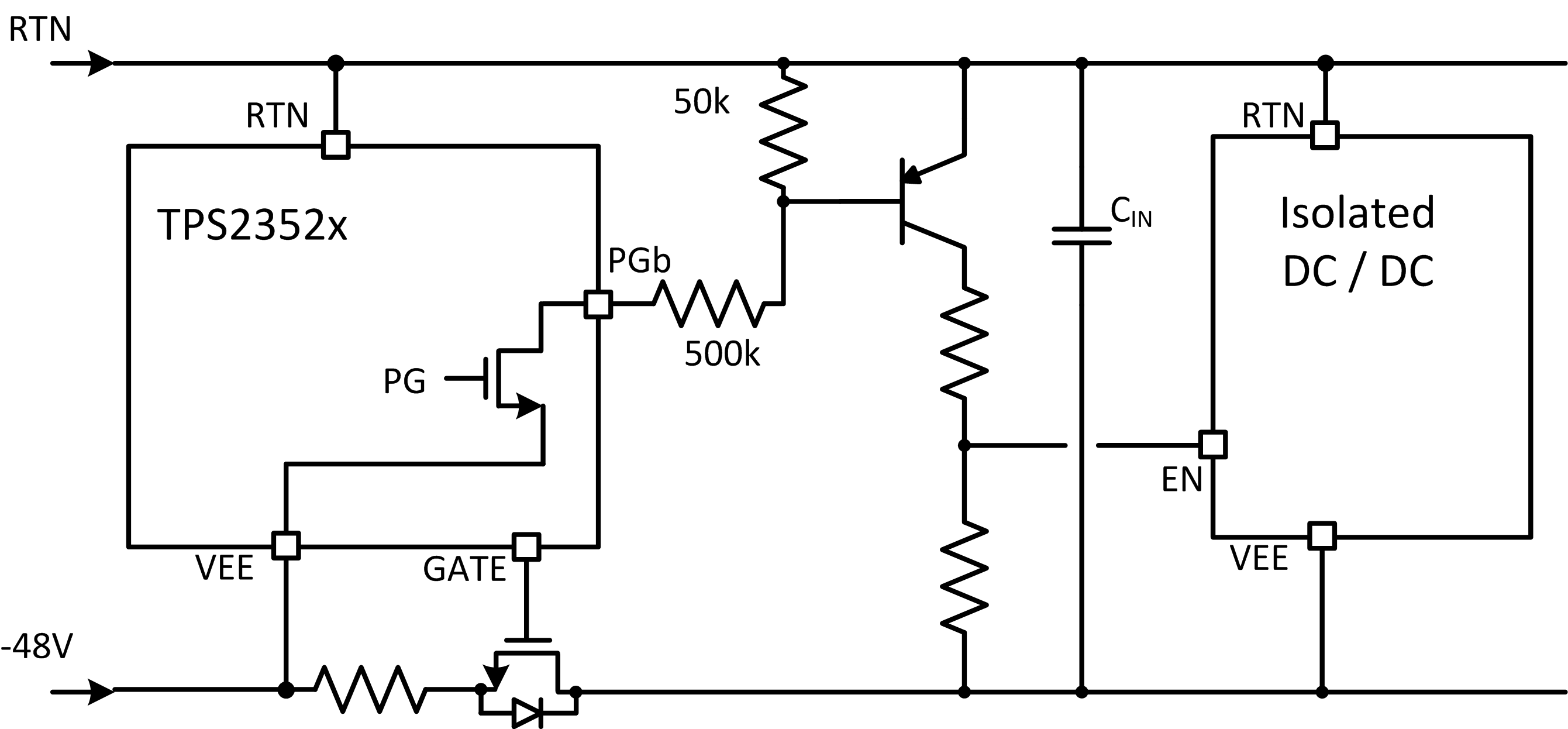
Power Good Interface to Downstream DC/DC

It is critical to keep the downstream DC/DC off while the hot swap is charging the bulk capacitor. This can be accomplished through the PGb pin. Note that the VEE of the hot swap and the DC/DC are different and the Power Good cannot be directly tied to the EN or UV of the DC/DC. The application circuit below provides a simple way to control the downstream converter with the PGb pin of the hot swap.
TPS23521 PGb_hook_up.pngFigure 14. Interface to DC/DC