JAJSF18A December 2017 – January 2019 TPS23523
PRODUCTION DATA.
- 1 特長
- 2 アプリケーション
- 3 概要
- 4 改訂履歴
- 5 Pin Configuration and Functions
- 6 Specifications
- 7 Parameter Measurement Information
- 8 Detailed Description
-
9 Application and Implementation
- 9.1 Application Information
- 9.2
Typical Application
- 9.2.1 Design Requirements
- 9.2.2
Detailed Design Procedure
- 9.2.2.1 Selecting RSNS
- 9.2.2.2 Selecting Soft Start Setting: CSS and CSS,VEE
- 9.2.2.3 Selecting VDS Switch Over Threshold
- 9.2.2.4 Timer Selection
- 9.2.2.5 MOSFET Selection and SOA Checks
- 9.2.2.6 Input Cap, Input TVS, and OR-ing FET selection
- 9.2.2.7 EMI Filter Consideration
- 9.2.2.8 Undervoltage and Overvoltage Settings
- 9.2.2.9 Choosing RVCC and CVCC
- 9.2.2.10 Power Good Interface to Downstream DC/DC
- 9.2.3 Application Curves
- 10Power Supply Recommendations
- 11Layout
- 12デバイスおよびドキュメントのサポート
- 13メカニカル、パッケージ、および注文情報
7.1 Relationship between Sense Voltage, Gate Current, and Timer
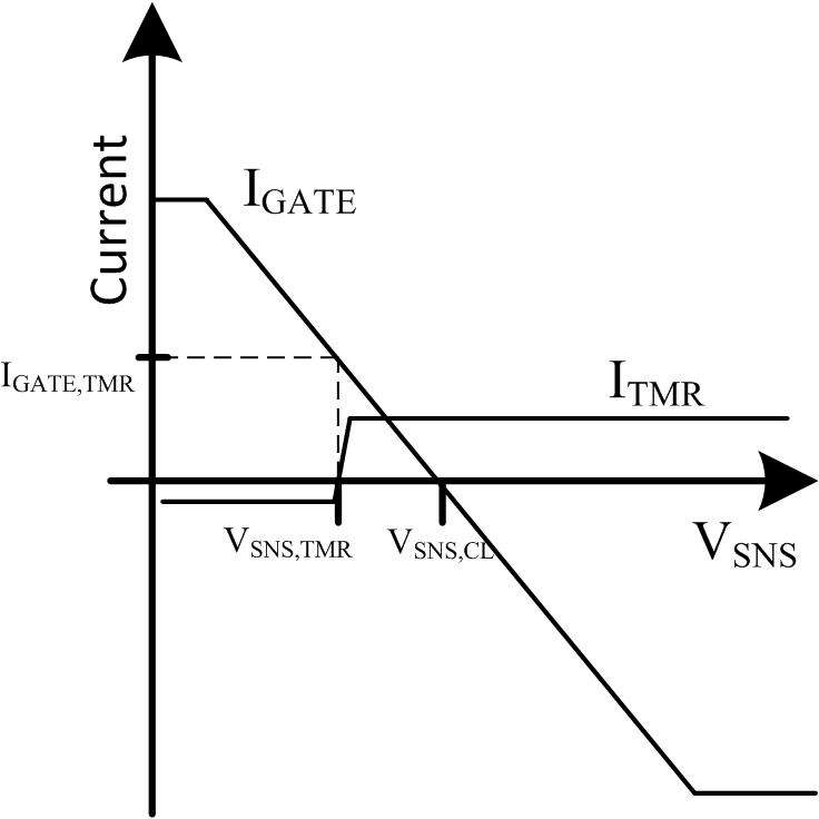
The diagram below illustrates the relationship between the VSNS (voltage across RSNS), Gate current, and the timer operation. The diagram is intended to help explain the various parameters in the electrical characteristic table and is not drawn to scale.
Note that IGATE reduces as the sense voltage approaches the current limit threshold and it equals zero at the current limit regulation point. To ensure that the timer always runs when the IC is in regulation the timer starts at a slightly positive IGATE.
 Figure 7. Relationship Between Timer, Gate Current, and Sense Voltage (VGATE = 5 V)