JAJSF18A December 2017 – January 2019 TPS23523
PRODUCTION DATA.
- 1 特長
- 2 アプリケーション
- 3 概要
- 4 改訂履歴
- 5 Pin Configuration and Functions
- 6 Specifications
- 7 Parameter Measurement Information
- 8 Detailed Description
-
9 Application and Implementation
- 9.1 Application Information
- 9.2
Typical Application
- 9.2.1 Design Requirements
- 9.2.2
Detailed Design Procedure
- 9.2.2.1 Selecting RSNS
- 9.2.2.2 Selecting Soft Start Setting: CSS and CSS,VEE
- 9.2.2.3 Selecting VDS Switch Over Threshold
- 9.2.2.4 Timer Selection
- 9.2.2.5 MOSFET Selection and SOA Checks
- 9.2.2.6 Input Cap, Input TVS, and OR-ing FET selection
- 9.2.2.7 EMI Filter Consideration
- 9.2.2.8 Undervoltage and Overvoltage Settings
- 9.2.2.9 Choosing RVCC and CVCC
- 9.2.2.10 Power Good Interface to Downstream DC/DC
- 9.2.3 Application Curves
- 10Power Supply Recommendations
- 11Layout
- 12デバイスおよびドキュメントのサポート
- 13メカニカル、パッケージ、および注文情報
9.2.2.5 MOSFET Selection and SOA Checks
When selecting MOSFETs for the –48 V application the three key parameters are: VDS rating, RDSON, and safe operating area (SOA). For this application the CSD19535KTT was selected to provide a 100 V VDS rating, low RDSON, and sufficient SOA. After selecting the MOSFET, it is important to double check that it has sufficient SOA to handle the key stress scenarios: start-up, output Hot Short, and Start into Short. MOSFET's SOA is usually specified at a case temperature of 25°C and should be derated based on the maximum case temperature expected in the application. Compute the maximum case temperature using the equation below. Note that the RDSON will vary with temperature and solving the equation below could be a repetitive process. The CSD19535KTT, has a maximum 3.4 mΩ RDSON at room temperature and is ~1.5x higher at 100°C. N stands for the number of MOSFETs used in parallel.


Next the stress the MOSFET will experience during operation should be compared to the FETs capability. First, consider the power up. The inrush current with max COUT will be 0.37 A and the inrush will last for 129 ms. Note that the power dissipation of the FET will start at VIN,MAX × IINR and reduce to zero as the VDS of the MOSFET is reduced. The SOA curve of a typical MOSFET assume the same power dissipation for a given time. A conservative approach is to assume an equivalent power profile where PFET = VIN,MAX × IINR for t = Tstart-up /2. In this instance, the SOA can be checked by looking at a 60 V, 0.4 A, 64.5 ms pulse. Based on the SOA of the CSD19535KTT, it can handle 60 V, 1.8 A for 10 ms and it can handle 60 V, 1 A for 100 ms. The SOA at TC = 25°C for 64.5 ms can be extrapolated by approximating SOA vs time as a power function as shown in equations below:


Finally, the FET SOA needs to be derated based on the maximum case temperature as shown below. Note that the FET can handle 0.59 A, while it will have 0.37 A during start-up. Thus there is a lot of margin during this test condition.

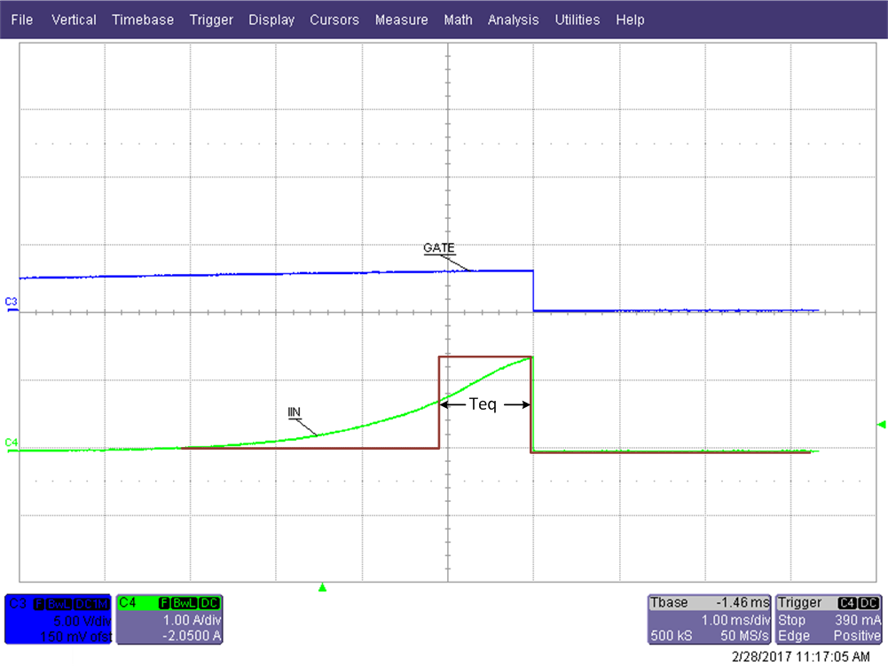
A similar approach should be taken to compute the FETs SOA capability during a Hot Short and start into short. As shown in the following figure, during a start into short the gate is coming up very slowly due to a large capacitance tied to the gate through the SS pin. Thus it is more stressful than a Hot Short and should be used for worst case SOA calculations. To compare the FET stress during start-up into short to the SOA curves the stress needs to be approximated as a square pulse as showing in the figure below. In this example, the stress is approximated with a 1.1 ms (Teq), 1.5 A, 60 V pulse. The FET can handle 6 A, 60 V for 1 ms and 1.8 A, 60 V for 10 ms. Using approximation and temp derating as shown earlier, the FET's capability can be computed as 3 A, 60 V, for 1.1 ms at 96°C. 3 A is significantly larger than 1.5 A implying good margin.
 Figure 15. Teq During a Start Into a Short
 The final operating point to check is the operation with high current and VDS just below the VDS,SW threshold. In this example, the time out would be 1.1ms (one half of the time out at Vd = 0 V), the current will be 12.5 A, and the voltage would be 20 V. Looking up the SOA curve, the FET can handle 30 A, 20 V for 1 ms and 10 A, 20 V for 10 ms. Repeating previously shown approximations and temp derating, the FET's capability is computed to be 16 A, 20 V, for 1.1 ms at 96°C. Again this is below the worst case operating point of 12.5 A and 20 V suggesting good margin.
