JAJSF18A December   2017  – January 2019 TPS23523

PRODUCTION DATA.  

  1. 特長
  2. アプリケーション
  3. 概要
    1.     Device Images
      1.      概略回路図
  4. 改訂履歴
  5. Pin Configuration and Functions
    1.     Pin Functions
  6. Specifications
    1. 6.1 Absolute Maximum Ratings
    2. 6.2 ESD Ratings
    3. 6.3 Recommended Operating Conditions
    4. 6.4 Thermal Information
    5. 6.5 Electrical Characteristics
    6. 6.6 Switching Characteristics
    7. 6.7 Typical Characteristics
  7. Parameter Measurement Information
    1. 7.1 Relationship between Sense Voltage, Gate Current, and Timer
  8. Detailed Description
    1. 8.1 Overview
    2. 8.2 Functional Block Diagram
    3. 8.3 Feature Description
      1. 8.3.1 Current Limit
        1. 8.3.1.1 Programming the CL Switch-Over Threshold
        2. 8.3.1.2 Setting Up the PROG Pin
        3. 8.3.1.3 Programming CL1
        4. 8.3.1.4 Programming CL2
      2. 8.3.2 Soft Start Disconnect
      3. 8.3.3 Timer
      4. 8.3.4 Gate 2
      5. 8.3.5 OR-ing
    4. 8.4 Device Functional Modes
      1. 8.4.1 OFF State
      2. 8.4.2 Insertion Delay State
      3. 8.4.3 Start-up State
      4. 8.4.4 Normal Operation State
  9. Application and Implementation
    1. 9.1 Application Information
    2. 9.2 Typical Application
      1. 9.2.1 Design Requirements
      2. 9.2.2 Detailed Design Procedure
        1. 9.2.2.1  Selecting RSNS
        2. 9.2.2.2  Selecting Soft Start Setting: CSS and CSS,VEE
        3. 9.2.2.3  Selecting VDS Switch Over Threshold
        4. 9.2.2.4  Timer Selection
        5. 9.2.2.5  MOSFET Selection and SOA Checks
        6. 9.2.2.6  Input Cap, Input TVS, and OR-ing FET selection
        7. 9.2.2.7  EMI Filter Consideration
        8. 9.2.2.8  Undervoltage and Overvoltage Settings
        9. 9.2.2.9  Choosing RVCC and CVCC
        10. 9.2.2.10 Power Good Interface to Downstream DC/DC
      3. 9.2.3 Application Curves
  10. 10Power Supply Recommendations
  11. 11Layout
    1. 11.1 Layout Guidelines
    2. 11.2 Layout Example
  12. 12デバイスおよびドキュメントのサポート
    1. 12.1 デバイス・サポート
      1. 12.1.1 デベロッパー・ネットワークの製品に関する免責事項
    2. 12.2 ドキュメントのサポート
      1. 12.2.1 関連資料
    3. 12.3 ドキュメントの更新通知を受け取る方法
    4. 12.4 コミュニティ・リソース
    5. 12.5 商標
    6. 12.6 静電気放電に関する注意事項
    7. 12.7 Glossary
  13. 13メカニカル、パッケージ、および注文情報

パッケージ・オプション

メカニカル・データ(パッケージ|ピン)
サーマルパッド・メカニカル・データ
発注情報

Application Curves

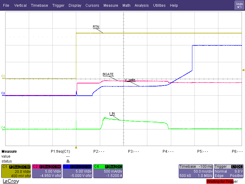
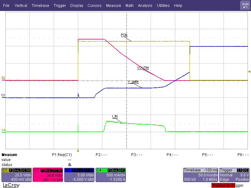
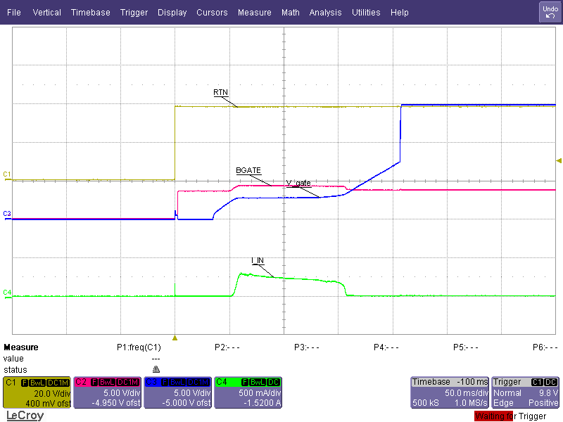
TPS23523 HotPlug54V.png
Figure 17. Start Up (Vin = 54 V)
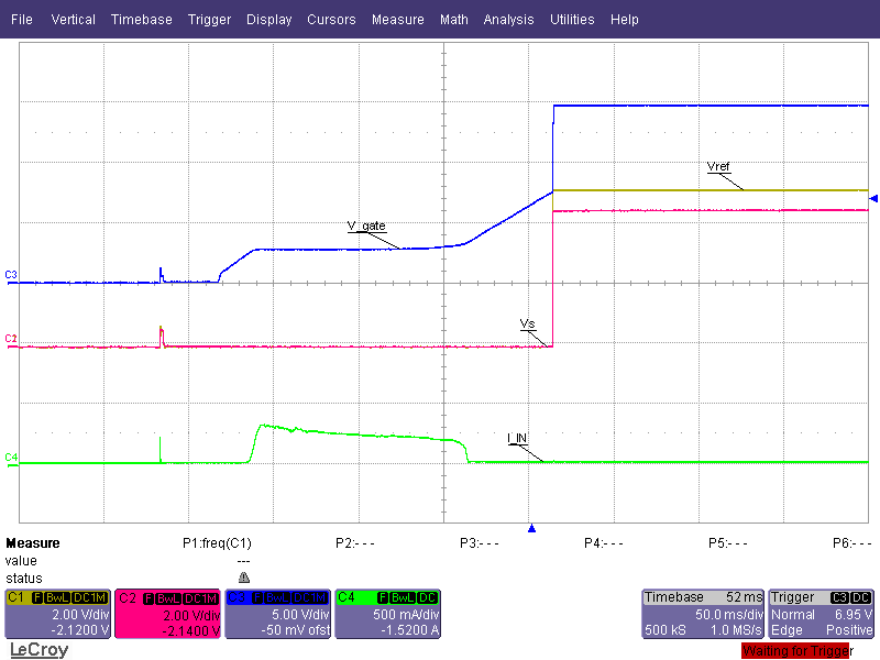
TPS23523 HotPlug54V_3.png
Figure 19. Start Up (Vin = 54 V)
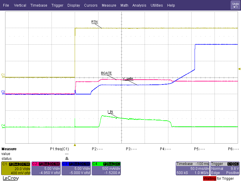
TPS23523 HotPlug60V.png
Figure 21. Start Up (Vin = 60 V)
TPS23523 HotShort_3.png
Zoomed In
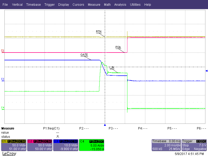
Figure 23. Hot Short (Vin = 54 V)
TPS23523 ILIM_LoadStep.png
Figure 25. Load Step Into Current Limit
TPS23523 StartIntoShort.png
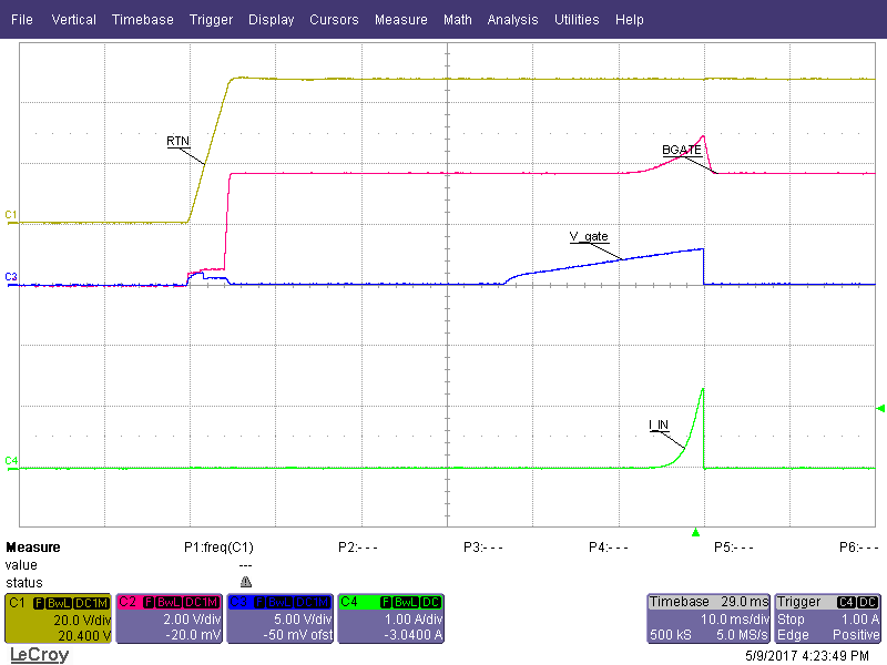
Figure 27. Start Into Short
TPS23523 VinShort.png
5-A load
Figure 29. Short on Vin
TPS23523 ReverseHookUp.png
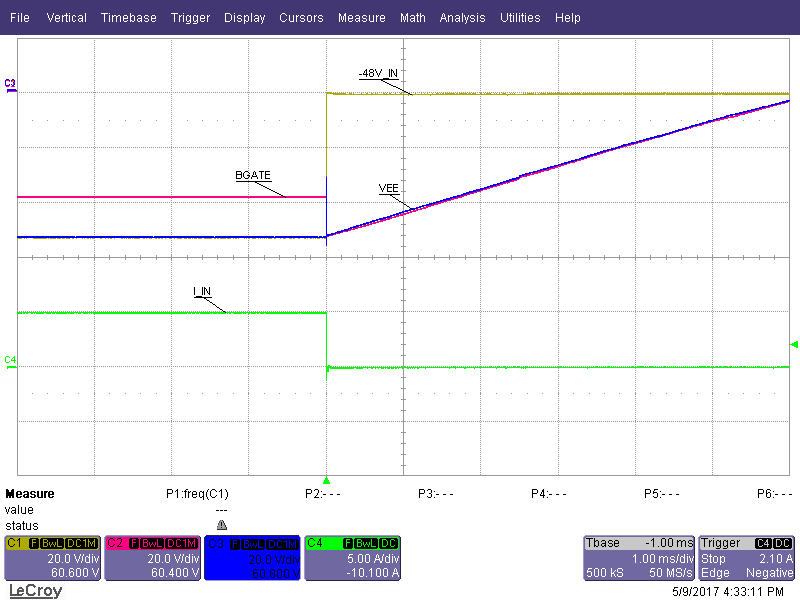
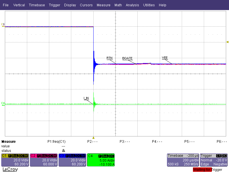
Figure 31. Reverse Hook Up
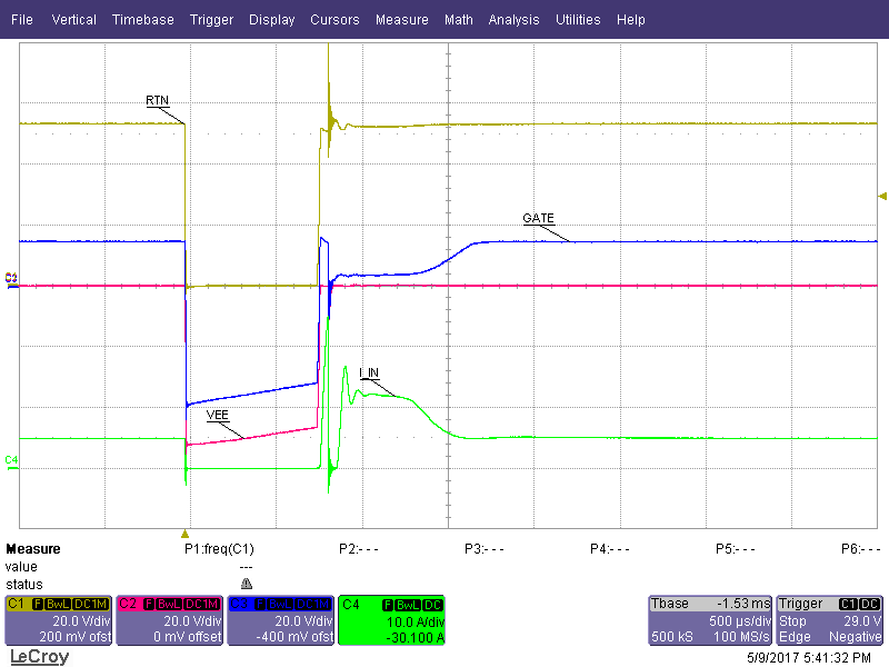
TPS23523 Brown_Out.png
5-A load
Figure 33. 1-ms Brown Out
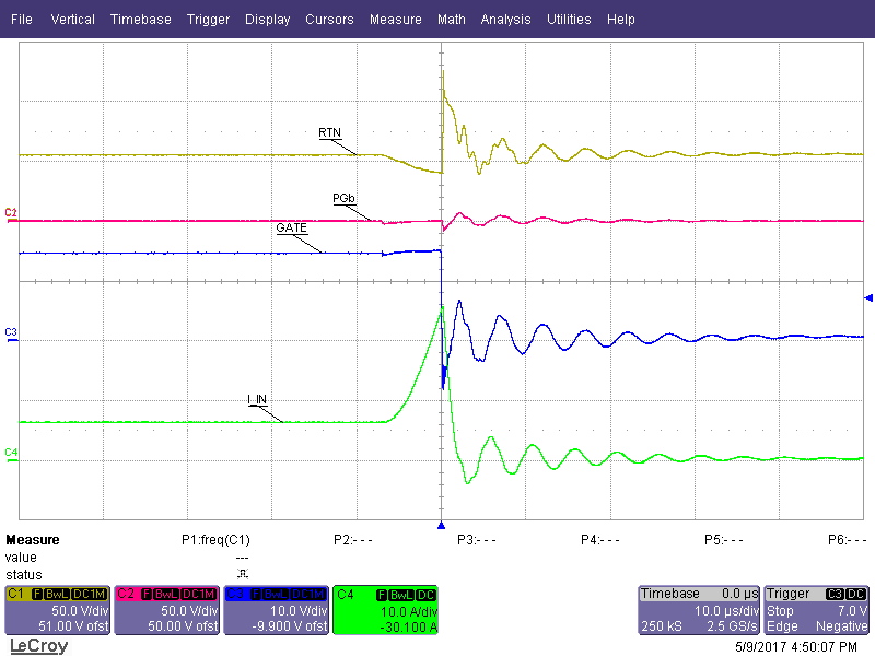
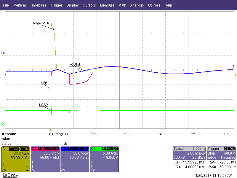
TPS23523 LightningSurge_2kV_2.png
6-A load, per IEC61000-4-5
Figure 35. 2 kV (2 Ω) Lightning Surge
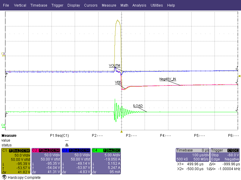
TPS23523 LightningSurge_Neg2kV_2.png
6-A load, per IEC61000-4-5
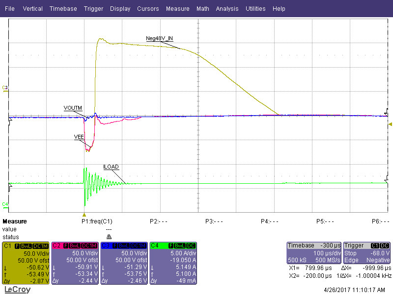
Figure 37. -2 kV (2 Ω) Lightning Surge
TPS23523 HotPlug54V_2.png
Figure 18. Start Up (Vin = 54 V)
TPS23523 HotPlug38V.png
Figure 20. Start Up (Vin = 38 V)
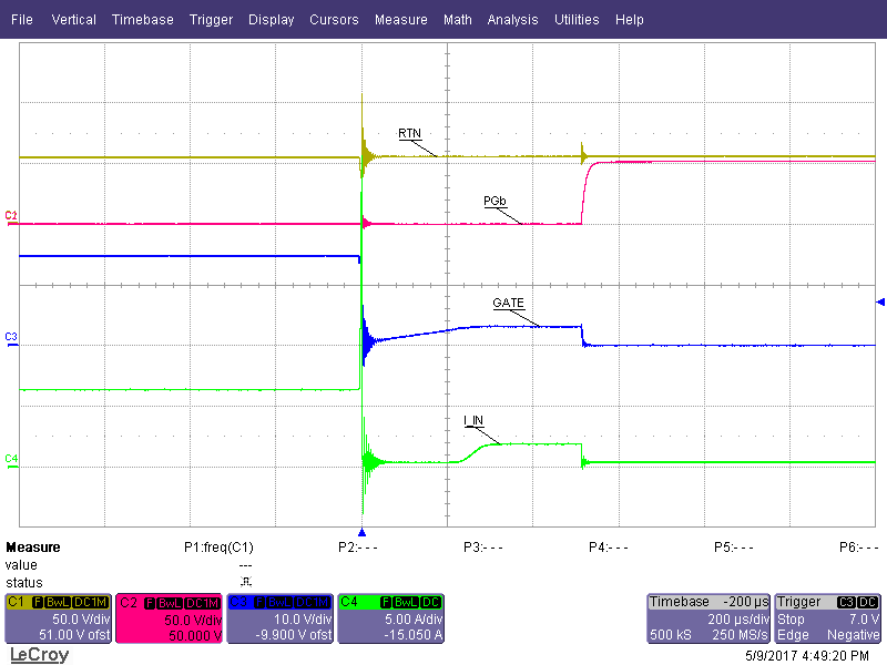
TPS23523 HotShort_2.png
Figure 22. Hot Short (Vin = 54 V)
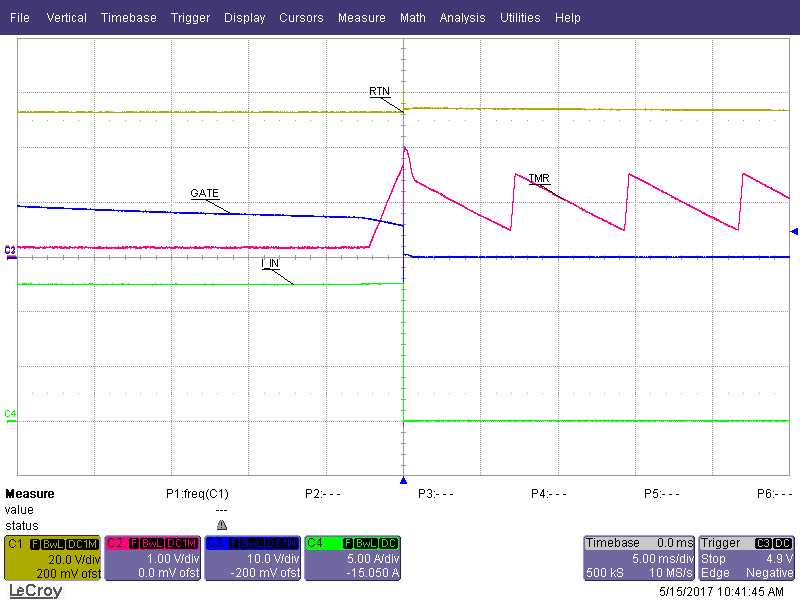
TPS23523 Gradual_OverCurrent.png
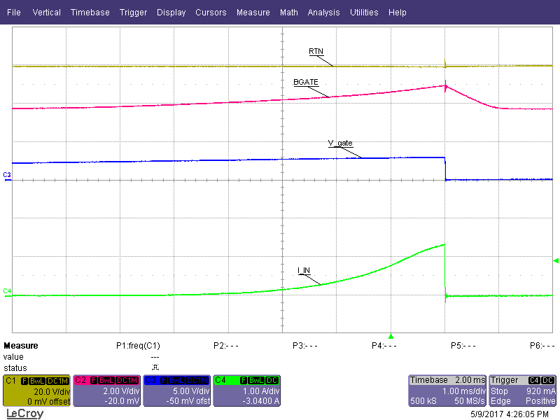
Figure 24. Gradual Over Current
TPS23523 IlimLoadStep_2.png
Figure 26. Load Step Into Current Limit
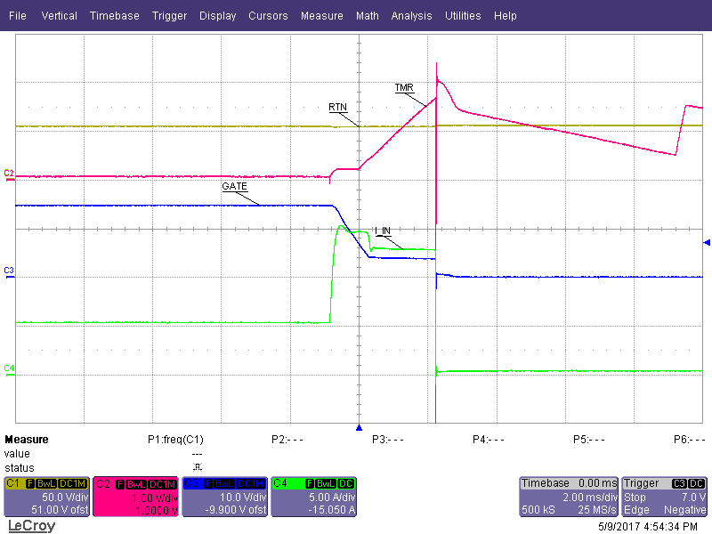
TPS23523 StartIntoShort_2.png
Figure 28. Start Into Short
TPS23523 VinShort_2.png
5-A load
Figure 30. Short on Vin
TPS23523 ReverseHookUp_2.png
Figure 32. Reverse Hook Up
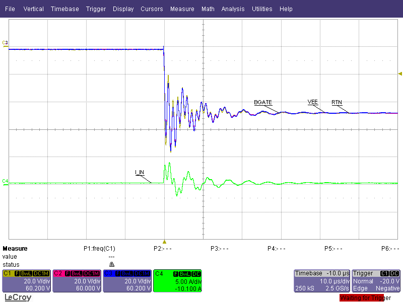
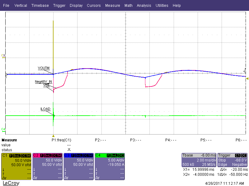
TPS23523 LightningSurge_2kV.png
6-A load, per IEC61000-4-5
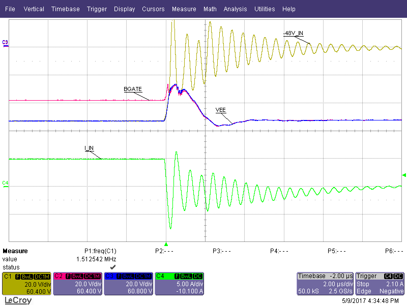
Figure 34. 2 kV (2 Ω) Lightning Surge
TPS23523 LightningSurge_Neg2kV.png
6-A load, per IEC61000-4-5
Figure 36. -2 kV (2 Ω) Lightning Surge