JAJSK02 October 2020 TPS23731
PRODUCTION DATA
- 1 特長
- 2 アプリケーション
- 3 概要
- 4 Revision History
- 5 Device Comparison Table
- 6 Pin Configuration and Functions
- 7 Specifications
-
8 Detailed Description
- 8.1 Overview
- 8.2 Functional Block Diagram
- 8.3
Feature Description
- 8.3.1 CLS Classification
- 8.3.2 DEN Detection and Enable
- 8.3.3 APD Auxiliary Power Detect
- 8.3.4 Internal Pass MOSFET
- 8.3.5 T2P and APDO Indicators
- 8.3.6
DC-DC Controller Features
- 8.3.6.1 VCC, VB, VBG and Advanced PWM Startup
- 27
- 8.3.6.2 CS, Current Slope Compensation and blanking
- 8.3.6.3 COMP, FB, EA_DIS, CP, PSRS and Opto-less Feedback
- 8.3.6.4 FRS Frequency Setting and Synchronization
- 8.3.6.5 DTHR and Frequency Dithering for Spread Spectrum Applications
- 8.3.6.6 SST and Soft-Start of the Switcher
- 8.3.6.7 SST, I_STP, LINEUV and Soft-Stop of the Switcher
- 8.3.7 Switching FET Driver - GATE
- 8.3.8 EMPS and Automatic MPS
- 8.3.9 VDD Supply Voltage
- 8.3.10 RTN, AGND, GND
- 8.3.11 VSS
- 8.3.12 Exposed Thermal pads - PAD_G and PAD_S
- 8.4
Device Functional Modes
- 8.4.1 PoE Overview
- 8.4.2 Threshold Voltages
- 8.4.3 PoE Start-Up Sequence
- 8.4.4 Detection
- 8.4.5 Hardware Classification
- 8.4.6 Maintain Power Signature (MPS)
- 8.4.7 Advanced Start-Up and Converter Operation
- 8.4.8 Line Undervoltage Protection and Converter Operation
- 8.4.9 PD Self-Protection
- 8.4.10 Thermal Shutdown - DC-DC Controller
- 8.4.11 Adapter ORing
-
9 Application and Implementation
- 9.1 Application Information
- 9.2
Typical Application
- 9.2.1
Design Requirements
- 9.2.1.1
Detailed Design Procedure
- 9.2.1.1.1 Input Bridges and Schottky Diodes
- 9.2.1.1.2 Input TVS Protection
- 9.2.1.1.3 Input Bypass Capacitor
- 9.2.1.1.4 Detection Resistor, RDEN
- 9.2.1.1.5 Classification Resistor, RCLS.
- 9.2.1.1.6 APD Pin Divider Network, RAPD1, RAPD2
- 9.2.1.1.7 Setting Frequency (RFRS) and Synchronization
- 9.2.1.1.8 Bias Supply Requirements and CVCC
- 9.2.1.1.9 APDO, T2P Interface
- 9.2.1.1.10 Output Voltage Feedback Divider, RAUX, R1,R2
- 9.2.1.1.11 Frequency Dithering for Conducted Emissions Control
- 9.2.1.1
Detailed Design Procedure
- 9.2.1
Design Requirements
- 10Power Supply Recommendations
- 11Layout
- 12Device and Documentation Support
- 13Mechanical, Packaging, and Orderable Information
8.4.9 PD Self-Protection
IEEE802.3bt includes new PSE output limiting requirements for Type 3 and 4 operation to cover higher power and 4-pair applications. Type 2, 3 and 4 PSEs must meet an output current vs time template with specified minimum and maximum sourcing boundaries. The peak output current per each 2-pair may be as high as 50 A for 10 μs or 1.75 A for 75 ms, and the total peak current becomes twice these values when power is delivered over 4 pairs. This makes robust protection of the PD device even more important than it was in IEEE 802.3-2012.
The PD section has the following self-protection functions.
- Hotswap switch current limit
- Hotswap switch foldback
- Hotswap thermal protection
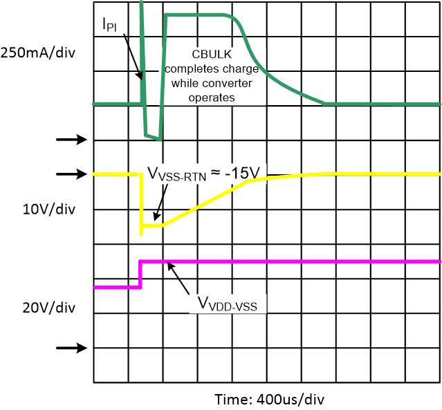
The internal hotswap MOSFET of the TPS23731 is protected against output faults and input voltage steps with a current limit and deglitched foldback. High stress conditions include converter output shorts, shorts from VDD to RTN, or transients on the input line. An overload on the pass MOSFET engages the current limit, with VRTN-VSS rising as a result. If VRTN rises above approximately 14.8 V for longer than approximately 1.8 ms, the current limit reverts to the inrush limit, and turns the converter off, although there is no minimum inrush delay period (84 ms) applicable in this case. The 1.8-ms deglitch feature prevents momentary transients from causing a PD reset, provided that recovery lies within the bounds of the hotswap and PSE protection. Figure 8-14 shows an example of recovery from a 15-V PSE rising voltage step. The hotswap MOSFET goes into current limit, overshooting to a relatively low current, recovers to 925-mA full current limit, and charges the input capacitor while the converter continues to run. The MOSFET did not go into foldback because VRTN-VSS was below 14.8 V after the 1.8-ms deglitch.
 Figure 8-14 Response to PSE Step Voltage
The PD control has a thermal sensor that protects the internal hotswap MOSFET. Conditions like start-up or operation into a VDD to RTN short cause high power dissipation in the MOSFET. An overtemperature shutdown (OTSD) turns off the hotswap MOSFET and class regulator, which are restarted after the device cools. The PD restarts in inrush phase when exiting from a PD overtemperature event.
Pulling DEN to VSS during powered operation causes the internal hotswap MOSFET to turn off. This feature allows a PD with secondary-side adapter ORing to achieve adapter priority. Take care with synchronous converter topologies that can deliver power in both directions.
The hotswap switch is forced off under the following conditions:
- VAPD above VAPDEN (approximately 1.5 V)
- VDEN ≤ VPD_DIS when VVDD-VSS is in the operational range
- PD over temperature
- VVDD-VSS < PoE UVLO (approximately 32 V)