JAJSK02 October 2020 TPS23731
PRODUCTION DATA
- 1 特長
- 2 アプリケーション
- 3 概要
- 4 Revision History
- 5 Device Comparison Table
- 6 Pin Configuration and Functions
- 7 Specifications
-
8 Detailed Description
- 8.1 Overview
- 8.2 Functional Block Diagram
- 8.3
Feature Description
- 8.3.1 CLS Classification
- 8.3.2 DEN Detection and Enable
- 8.3.3 APD Auxiliary Power Detect
- 8.3.4 Internal Pass MOSFET
- 8.3.5 T2P and APDO Indicators
- 8.3.6
DC-DC Controller Features
- 8.3.6.1 VCC, VB, VBG and Advanced PWM Startup
- 27
- 8.3.6.2 CS, Current Slope Compensation and blanking
- 8.3.6.3 COMP, FB, EA_DIS, CP, PSRS and Opto-less Feedback
- 8.3.6.4 FRS Frequency Setting and Synchronization
- 8.3.6.5 DTHR and Frequency Dithering for Spread Spectrum Applications
- 8.3.6.6 SST and Soft-Start of the Switcher
- 8.3.6.7 SST, I_STP, LINEUV and Soft-Stop of the Switcher
- 8.3.7 Switching FET Driver - GATE
- 8.3.8 EMPS and Automatic MPS
- 8.3.9 VDD Supply Voltage
- 8.3.10 RTN, AGND, GND
- 8.3.11 VSS
- 8.3.12 Exposed Thermal pads - PAD_G and PAD_S
- 8.4
Device Functional Modes
- 8.4.1 PoE Overview
- 8.4.2 Threshold Voltages
- 8.4.3 PoE Start-Up Sequence
- 8.4.4 Detection
- 8.4.5 Hardware Classification
- 8.4.6 Maintain Power Signature (MPS)
- 8.4.7 Advanced Start-Up and Converter Operation
- 8.4.8 Line Undervoltage Protection and Converter Operation
- 8.4.9 PD Self-Protection
- 8.4.10 Thermal Shutdown - DC-DC Controller
- 8.4.11 Adapter ORing
-
9 Application and Implementation
- 9.1 Application Information
- 9.2
Typical Application
- 9.2.1
Design Requirements
- 9.2.1.1
Detailed Design Procedure
- 9.2.1.1.1 Input Bridges and Schottky Diodes
- 9.2.1.1.2 Input TVS Protection
- 9.2.1.1.3 Input Bypass Capacitor
- 9.2.1.1.4 Detection Resistor, RDEN
- 9.2.1.1.5 Classification Resistor, RCLS.
- 9.2.1.1.6 APD Pin Divider Network, RAPD1, RAPD2
- 9.2.1.1.7 Setting Frequency (RFRS) and Synchronization
- 9.2.1.1.8 Bias Supply Requirements and CVCC
- 9.2.1.1.9 APDO, T2P Interface
- 9.2.1.1.10 Output Voltage Feedback Divider, RAUX, R1,R2
- 9.2.1.1.11 Frequency Dithering for Conducted Emissions Control
- 9.2.1.1
Detailed Design Procedure
- 9.2.1
Design Requirements
- 10Power Supply Recommendations
- 11Layout
- 12Device and Documentation Support
- 13Mechanical, Packaging, and Orderable Information
8.3.6.1 VCC, VB, VBG and Advanced PWM Startup
The VCC pin connects to the auxiliary bias supply for the DC-DC controller. The switching MOSFET gate driver draws current directly from the VCC pin. VB and VBG outputs are regulated down from VCC voltage, the former providing power to the internal control circuitry and external feedback optocoupler (when in use), and the latter providing power to the switching FET gate predriver circuit. A startup current source from VDD to VCC implements the converter bootstrap startup. VCC must receive power from an auxiliary source, such as an auxiliary winding on the flyback transformer, to sustain normal operation after startup.
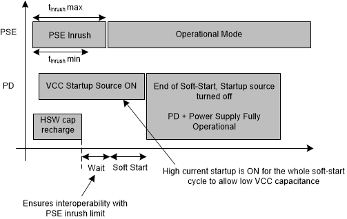
The startup current source is turned on during the inrush phase, charging CVCC and maintaining its voltage, and it is turned off only after the DC-DC soft-start cycle has been completed, which occurs when the DC-DC converter has ramped up its output voltage and VSST has exceed approximately 2.1 V (VSTUOF), as shown in Figure 8-1. Internal loading on VCC, VB and VBG is initially minimal while CVCC charges, to allow the converter to start. Due to the high current capability of the startup source, the recommended capacitance at VCC is relatively small, typically 1 μF in most applications.
Once VVCC falls below its UVLO threshold (VCUVLO_F, approximately 6.1 V), the converter shuts off and the startup current source is turned back on, initiating a new PWM startup cycle.
If however a VVCC fall (below approximately 7.1 V) is due to a light load condition causing temporary switching stop, the startup is immediately and for a short period turned back on to bring VCC voltage back up, with no converter interruption.
 Figure 8-1 Advanced Startup