JAJSK02 October 2020 TPS23731
PRODUCTION DATA
- 1 特長
- 2 アプリケーション
- 3 概要
- 4 Revision History
- 5 Device Comparison Table
- 6 Pin Configuration and Functions
- 7 Specifications
-
8 Detailed Description
- 8.1 Overview
- 8.2 Functional Block Diagram
- 8.3
Feature Description
- 8.3.1 CLS Classification
- 8.3.2 DEN Detection and Enable
- 8.3.3 APD Auxiliary Power Detect
- 8.3.4 Internal Pass MOSFET
- 8.3.5 T2P and APDO Indicators
- 8.3.6
DC-DC Controller Features
- 8.3.6.1 VCC, VB, VBG and Advanced PWM Startup
- 27
- 8.3.6.2 CS, Current Slope Compensation and blanking
- 8.3.6.3 COMP, FB, EA_DIS, CP, PSRS and Opto-less Feedback
- 8.3.6.4 FRS Frequency Setting and Synchronization
- 8.3.6.5 DTHR and Frequency Dithering for Spread Spectrum Applications
- 8.3.6.6 SST and Soft-Start of the Switcher
- 8.3.6.7 SST, I_STP, LINEUV and Soft-Stop of the Switcher
- 8.3.7 Switching FET Driver - GATE
- 8.3.8 EMPS and Automatic MPS
- 8.3.9 VDD Supply Voltage
- 8.3.10 RTN, AGND, GND
- 8.3.11 VSS
- 8.3.12 Exposed Thermal pads - PAD_G and PAD_S
- 8.4
Device Functional Modes
- 8.4.1 PoE Overview
- 8.4.2 Threshold Voltages
- 8.4.3 PoE Start-Up Sequence
- 8.4.4 Detection
- 8.4.5 Hardware Classification
- 8.4.6 Maintain Power Signature (MPS)
- 8.4.7 Advanced Start-Up and Converter Operation
- 8.4.8 Line Undervoltage Protection and Converter Operation
- 8.4.9 PD Self-Protection
- 8.4.10 Thermal Shutdown - DC-DC Controller
- 8.4.11 Adapter ORing
-
9 Application and Implementation
- 9.1 Application Information
- 9.2
Typical Application
- 9.2.1
Design Requirements
- 9.2.1.1
Detailed Design Procedure
- 9.2.1.1.1 Input Bridges and Schottky Diodes
- 9.2.1.1.2 Input TVS Protection
- 9.2.1.1.3 Input Bypass Capacitor
- 9.2.1.1.4 Detection Resistor, RDEN
- 9.2.1.1.5 Classification Resistor, RCLS.
- 9.2.1.1.6 APD Pin Divider Network, RAPD1, RAPD2
- 9.2.1.1.7 Setting Frequency (RFRS) and Synchronization
- 9.2.1.1.8 Bias Supply Requirements and CVCC
- 9.2.1.1.9 APDO, T2P Interface
- 9.2.1.1.10 Output Voltage Feedback Divider, RAUX, R1,R2
- 9.2.1.1.11 Frequency Dithering for Conducted Emissions Control
- 9.2.1.1
Detailed Design Procedure
- 9.2.1
Design Requirements
- 10Power Supply Recommendations
- 11Layout
- 12Device and Documentation Support
- 13Mechanical, Packaging, and Orderable Information
8.4.5 Hardware Classification
Hardware classification allows a PSE to determine a PD’s power requirements before powering, and helps with power management once power is applied. Type 2, 3, and 4 hardware classification permits high power PDs to determine whether the PSE can support its high-power operation. The number of class cycles generated by the PSE prior to turn on indicates to the PD if it allots the power requested or if the allocated power is less than requested, in which case there is power demotion.
A Type 2 PD always presents Class 4 in hardware to indicate that it is a 25.5W device. A Class 5 or 6 Type 3 PD presents Class 4 in hardware during the first two class events and it presents Class 0 or 1, respectively, for all subsequent class events. A Class 7 or 8 Type 4 PD presents Class 4 in hardware during the first two class events and it presents Class 2 or 3, respectively, for all subsequent class events. A Type 1 PSE will treat a Class 4 to 8 device like a Class 0 device, allotting 13 W if it chooses to power the PD. A Type 2 PSE will treat a Class 5 to 8 device like a Class 4 device, allotting 25.5W if it chooses to power the PD. A Class 4 PD that receives a 2-event class, a Class 5 or 6 PD that receives a 4-event class, or a Class 7 or 8 PD that receives a 5-event class, understands that the PSE has agreed to allocate the PD requested power. In the case where there is power demotion, the PD may choose to not start, or to start while not drawing more power than initially allocated, and request more power through the DLL after startup. The standard requires a Type 2, 3 or 4 PD to indicate that it is underpowered if this occurs. Startup of a high-power PD at lower power than requested implicitly requires some form of powering down sections of the application circuits.
The maximum power entries in Table 8-1 determine the class the PD must advertise. The PSE may disconnect a PD if it draws more than its stated class power, which may be the hardware class or a DLL-derived power level. The standard permits the PD to draw limited current peaks that increase the instantaneous power above the Table 8-1 limit; however, the average power requirement always applies.
The TPS23731 implements one- to two-event classification. RCLS resistor value defines the class of the PD. DLL communication is implemented by the Ethernet communication system in the PD and is not implemented by the TPS23731.
The TPS23731 disables classification above VCU_OFF to avoid excessive power dissipation. CLS voltage is turned off during PD thermal limiting or when APD or DEN is active. The CLS output is inherently current-limited, but should not be shorted to VSS for long periods of time.
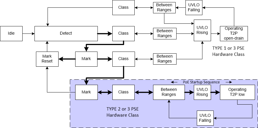
Figure 8-8 shows how classification works for the TPS23731. Transition from state-to-state occurs when comparator thresholds are crossed (see Figure 8-5 and Figure 8-6). These comparators have hysteresis, which adds inherent memory to the machine. Operation begins at idle (unpowered by PSE) and proceeds with increasing voltage from left to right. A 2-event classification follows the (heavy lined) path towards the bottom, ending up with a low T2P along the lower branch that is highlighted. Once the valid path to the PSE detection is broken, the input voltage must transition below the mark reset threshold to start anew.
 Figure 8-8 Up to Two-Event Class Internal States