SLVSB98A March 2012 – July 2015 TPS2379
PRODUCTION DATA.
- 1 Features
- 2 Applications
- 3 Description
- 4 Revision History
- 5 Pin Configuration and Functions
- 6 Specifications
- 7 Parameter Measurement Information
-
8 Detailed Description
- 8.1 Overview
- 8.2 Functional Block Diagram
- 8.3 Feature Description
- 8.4
Device Functional Modes
- 8.4.1
PoE Overview
- 8.4.1.1 Threshold Voltages
- 8.4.1.2 PoE Start-Up Sequence
- 8.4.1.3 Detection
- 8.4.1.4 Hardware Classification
- 8.4.1.5 Inrush and Start-up
- 8.4.1.6 Maintain Power Signature
- 8.4.1.7 Start-up and Operation
- 8.4.1.8 PD Hotswap Operation
- 8.4.1.9 CDB and T2P
- 8.4.1.10 Auxiliary Pass MOSFET Control
- 8.4.1.11 Using DEN to Disable PoE
- 8.4.1
PoE Overview
- 9 Application and Implementation
- 10Power Supply Recommendations
- 11Layout
- 12Device and Documentation Support
- 13Mechanical, Packaging, and Orderable Information
パッケージ・オプション
メカニカル・データ(パッケージ|ピン)
- DDA|8
サーマルパッド・メカニカル・データ
- DDA|8
発注情報
9 Application and Implementation
NOTE
Information in the following applications sections is not part of the TI component specification, and TI does not warrant its accuracy or completeness. TI’s customers are responsible for determining suitability of components for their purposes. Customers should validate and test their design implementation to confirm system functionality.
9.1 Application Information
The TPS2379 has the flexibility to be implemented in IEEE802.3at PDs, Universal Power Over Ethernet (UPOE) PDs, or high power non-standard PDs. Therefore, it can be used in a wide range applications such as video and VoIP telephones, multiband access points, security cameras, and pico-base stations.
9.2 Typical Application
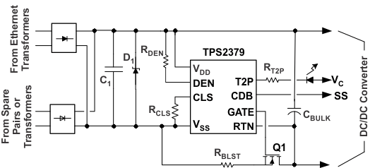
 Figure 26. Typical Application Circuit
9.2.1 Design Requirements
Table 3. TPS2379EVM Electrical and Performance Specifications
| PARAMETER | TEST CONDITIONS | MIN | TYP | MAX | UNIT |
|---|---|---|---|---|---|
| POWER INTERFACE | |||||
| Input voltage | Applied to the power pins of connectors J1 or J3 | 0 | 57 | V | |
| Operating voltage | After start-up | 30 | 57 | V | |
| Input UVLO | Rising input voltage at device terminals | 40 | V | ||
| Falling input voltage | 30.5 | ||||
| Detection voltage | At device terminals | 1.4 | 10.1 | V | |
| Classification voltage | At device terminals | 11.9 | 23 | V | |
| Detection signature | 24.9 | kΩ | |||
| Classification current | Class 4 | 38 | 42 | mA | |
| Inrush current limit | 100 | 180 | mA | ||
| Operating current limit | Internal plus external | 2260 | mA | ||
9.2.2 Detailed Design Procedures
Given in Equation 5, RBLST can be calulated using Equation 4

FMMT493TC can be used for Q2.
9.2.2.1 Input Bridges and Schottky Diodes
Using Schottky diodes instead of PN junction diodes for the PoE input bridges will reduce the power dissipation in these devices by about 30%. There are, however, some things to consider when using them.
The IEEE standard specifies a maximum backfeed voltage of 2.8 V. A 100 kΩ resistor is placed between the unpowered pairs and the voltage is measured across the resistor. Schottky diodes often have a higher reverse leakage current than PN diodes, making this a harder requirement to meet. To compensate, use conservative design for diode operating temperature, select lower-leakage devices where possible, and match leakage and temperatures by using packaged bridges.
Schottky diode leakage currents and lower dynamic resistances can impact the detection signature. Setting reasonable expectations for the temperature range over which the detection signature is accurate is the simplest solution. Increasing RDEN slightly may also help meet the requirement.
Schottky diodes have proven less robust to the stresses of ESD transients than PN junction diodes. After exposure to ESD, Schottky diodes may become shorted or leak. Take care to provide adequate protection in line with the exposure levels. This protection may be as simple as ferrite beads and capacitors.
As a general recommendation, use 1 A or 2 A, 100 V rated discrete or bridge diodes for the input rectifiers.
9.2.2.2 Protection, D1
A TVS, D1, across the rectified PoE voltage per Figure 26 must be used. A SMAJ58A, or equivalent, is recommended for general indoor applications. Adequate capacitive filtering or a TVS must limit input transient voltage to within the absolute maximum ratings. Outdoor transient levels or special applications require additional protection.
9.2.2.3 Capacitor, C1
The IEEE 802.3at standard specifies an input bypass capacitor (from VDD to VSS) of 0.05 μF to 0.12 μF. Typically a 0.1 μF, 100 V, 10% ceramic capacitor is used.
9.2.2.4 Detection Resistor, RDEN
The IEEE 802.3at standard specifies a detection signature resistance, RDEN between 23.75 kΩ and 26.25 kΩ, or 25 kΩ ± 5%. A resistor of 24.9 kΩ ± 1% is recommended for RDEN.
9.2.2.5 Classification Resistor, RCLS
Select RCLS according to Table 1. For Class 4, choose RCLS = 63.4 Ω.
9.2.2.6 External Boost Circuit
For a PD application requiring current limit of 2.26 A at the PD input (approximately 96 W) and using Q1 FET BUK7275-100A

9.2.3 Application Curves
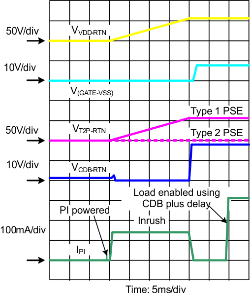
 Figure 27. Power Up and Start
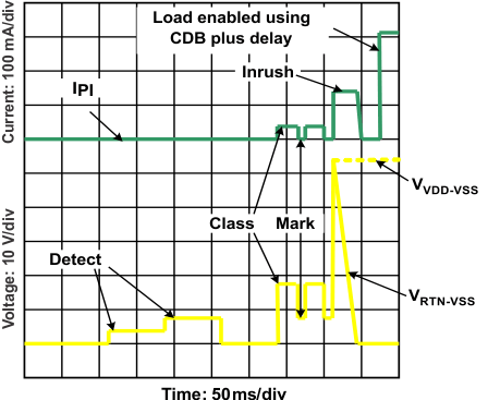
 Figure 28. Start-up