JAJSC25I March 2014 – July 2019 TPS23861
PRODUCTION DATA.
- 1 特長
- 2 アプリケーション
- 3 概要
- 4 改訂履歴
- 5 概要(続き)
- 6 Pin Configuration and Functions
- 7 Specifications
-
8 Detailed Description
- 8.1 Overview
- 8.2 Functional Block Diagram
- 8.3
Feature Description
- 8.3.1 Detection Resistance Measurement
- 8.3.2 Physical Layer Classification
- 8.3.3 Class and Detect Fields
- 8.3.4 Register State Following a Fault
- 8.3.5 Disconnect
- 8.3.6 Disconnect Threshold
- 8.3.7 Fast Shutdown Mode
- 8.3.8 Legacy Device Detection
- 8.3.9 VPWR Undervoltage and UVLO Events
- 8.3.10 Timer-Deferrable Interrupt Support
- 8.3.11 A/D Converter and I2C Interface
- 8.3.12 Independent Operation when the AUTO Bit is Set
- 8.3.13 I2C Slave Address and AUTO Bit Programming
- 8.4 Device Functional Modes
- 8.5
Register Map – I2C-Addressable
- 8.5.1 Interrupt Register
- 8.5.2 Interrupt Enable Register
- 8.5.3 Power Event Register
- 8.5.4 Detection Event Register
- 8.5.5 Fault Event Register
- 8.5.6 Start/ILIM Event Register
- 8.5.7 Supply Event Register
- 8.5.8 Port n Status Register
- 8.5.9 Power Status Register
- 8.5.10 I2C Slave Address Register
- 8.5.11 Operating Mode Register
- 8.5.12 Disconnect Enable Register
- 8.5.13 Detect/Class Enable Register
- 8.5.14 Port Power Priority Register
- 8.5.15 Timing Configuration Register
- 8.5.16 General Mask 1 Register
- 8.5.17 Detect/Class Restart Register
- 8.5.18 Power Enable Register
- 8.5.19 Reset Register
- 8.5.20 Legacy Detect Mode Register
- 8.5.21 Two-Event Classification Register
- 8.5.22 Interrupt Timer Register
- 8.5.23 Disconnect Threshold Register
- 8.5.24 ICUTnm CONFIG Register
- 8.5.25 Temperature Register
- 8.5.26 Input Voltage Register
- 8.5.27 Port n Current Register
- 8.5.28 Port n Voltage Register
- 8.5.29 PoE Plus Register
- 8.5.30 Firmware Revision Register
- 8.5.31 I2C Watchdog Register
- 8.5.32 Device ID Register
- 8.5.33 Cool Down/Gate Drive Register
- 8.5.34 Port n Detect Resistance Register
- 8.5.35 Port n Detect Voltage Difference Register
- 8.5.36 Reserved Registers
-
9 Application and Implementation
- 9.1 Introduction to PoE
- 9.2 Application Information
- 9.3 Typical Application
- 9.4 System Examples
- 10Power Supply Recommendations
- 11Layout
- 12デバイスおよびドキュメントのサポート
- 13メカニカル、パッケージ、および注文情報
8.3.13 I2C Slave Address and AUTO Bit Programming
NOTE
When using the I2C interface the host software should wait 22 ms minimum after a reset to ensure valid I2C transactions.
NOTE
Please note EEPROM endurance of 25 write cycles. Writing to the EEPROM more than this may result in erratic behavior.
The TPS23861 includes a means to program in EEPROM the following two fields:
- A seven bit I2C slave address for operation with a host processor.
- AUTO bit which allows the TPS23861 to operate independently without a host processor.
The benefits this approach include:
- Up to 125 similar devices become addressable.
- Provides a high level of flexibility.
- Helps to resolve conflicts with other peripherals on same I2C bus.
- The I2C address can be programmed at production subassembly module level or motherboard level.
- Allows a simple approach to field-installed upgrades or expansions to PSE systems.
- No physical address line required, no bank selection required.
- Smaller package. No address line pins and no AUTO pin.
NOTE
For compatibility with legacy systems, the module A3 bank addressing is provided by use of the A3 input pin.
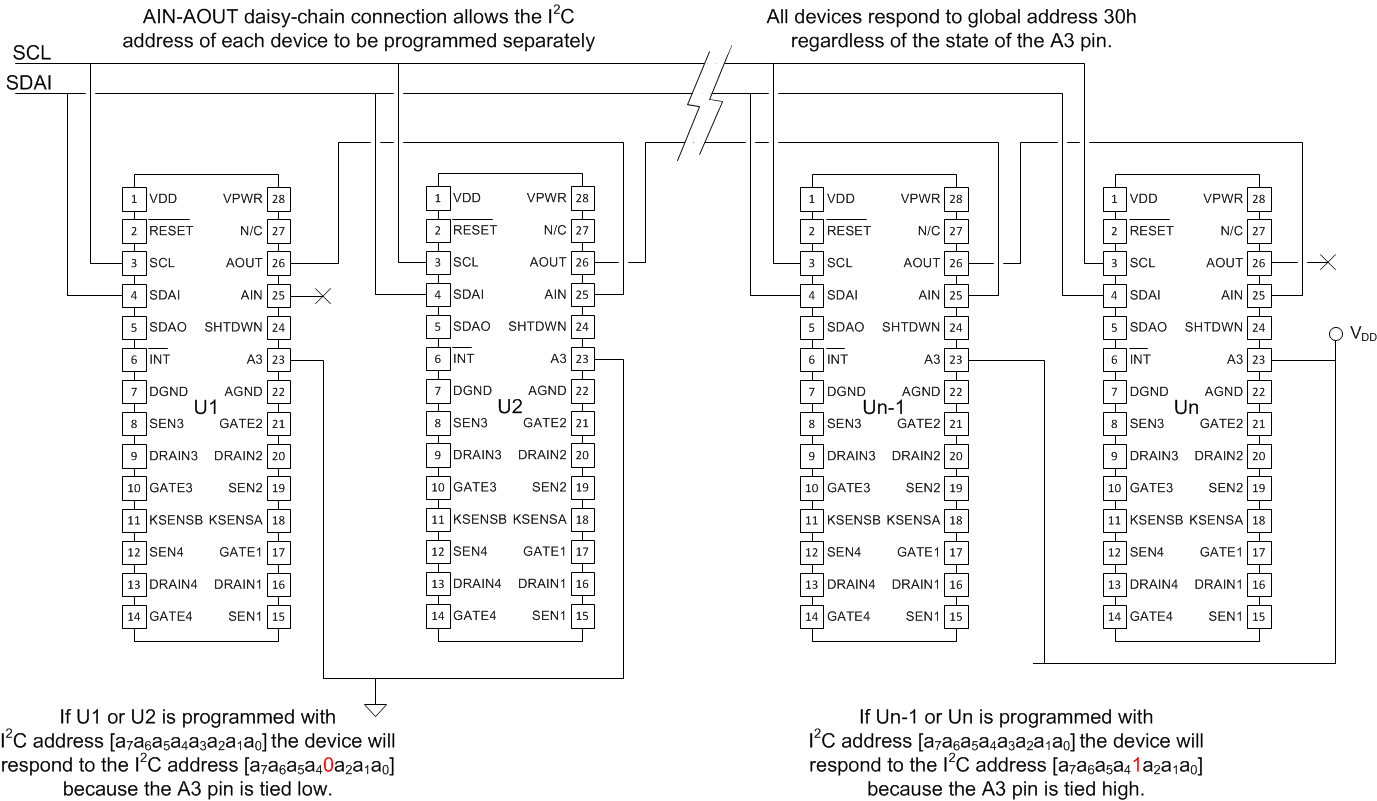
As shown in Figure 41, the initial I2C address programming access is established by a local daisy chain chip select connection between multiple TPS23861 devices. The AIN pin plays the role of a “moving chip select” during address programming.
NOTE
Global write command including an unlock code (AAh) is required in order to write to the I2C slave address register.
 Figure 41. I2C Slave Address and AUTO Bit Programming Circuit
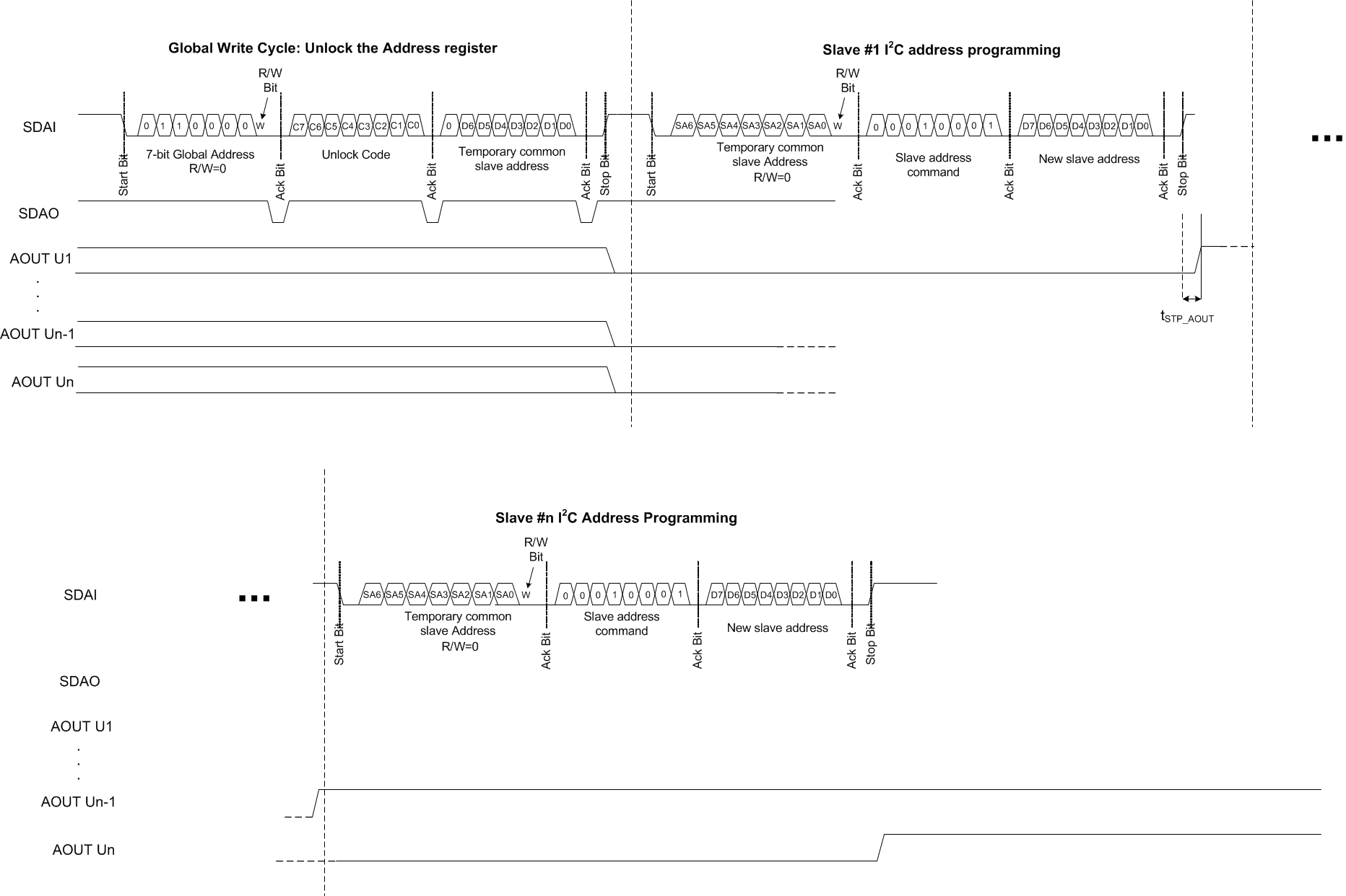
 The sequence during address programming is as follows:
- Global write command including an unlock code (AAh) and a temporary common slave address (any address other than 30h) is sent to all I2C devices through the broadcast address, 30h.
- All TPS23861 devices respond to the broadcast address 30h regardless of the state of the A3 pin. When the three-byte sequence is correctly decoded,
- Each TPS23861 has a new I2C address determined by the programmed temporary slave address with bit 3 equal to the state of the A3 pin.
- All TPS23861 devices force low the AOUT output.
- The first TPS23861 device being selected is the only one having its AIN pin at logic high level (U1 in Figure 41).
- Using the temporary slave address, write the new 7-bit device address in the I2C slave address register. See data format below.
- The first slave accepts the new address, then forces its AOUT output pin to high level and automatically locks the access to its slave address register. It also stores permanently its new slave address into EEPROM.
- The same procedure is repeated for the next slave device, which has just detected that its AIN input has become high.
- This is repeated until all slaves have been reprogrammed.
- The host can then interrogate each slave, one by one, in order to validate their new address.
- Bit 7 of the 8-bit transfer (AUTO) defines if the controller operates independently (no host processor) as an automatic PSE. The state of this bit is monitored only immediately following a power-on reset, writing a 1 to the RESAL bit of the RESET register, or after the RESET input has been activated. The impact of that bit state on registers after reset is reflected in the Table 10 (Reset State column) and is referred to as “A”.
NOTE
The SLA3 slave address bit follows the logic level of A3 input pin, as detailed for I2C Slave Address register.
| BITS | D7 | D6 | D5 | D4 | D3 | D2 | D1 | D0 |
|---|---|---|---|---|---|---|---|---|
| BIT NAME | AUTO | 7-bit I2C Address | ||||||
NOTE
During the address programming procedure if the slave has not received its new address within a timeout period (around 100 ms), it goes back to the initial slave address (before the address programming sequence was initiated); it locks its address register and releases its AOUT output.
NOTE
After programming a new I2C slave address to register 0×11, a 100 ms delay is recommended before trying to perform a read check.
NOTE
When using I2C scan for device discovery, it is recommended to add at least a 100 ms delay between writing commands to address 0x30 (Broadcast address) and 0x31. This prevents receiving unnecessary extra ACK. Skipping writing command to address 0x30 can also avoid the extra ACK.

