SLUSC25A February   2015  – August 2017 TPS2388

PRODUCTION DATA.  

  1. Features
  2. Applications
  3. Description
    1.     Device Images
      1.      Simplified Schematic
  4. Revision History
  5. Pin Configuration and Functions
    1.     Pin Functions
    2. 5.1 Detailed Pin Description
  6. Specifications
    1. 6.1 Absolute Maximum Ratings
    2. 6.2 ESD Ratings
    3. 6.3 Recommended Operating Conditions
    4. 6.4 Thermal Information
    5. 6.5 Electrical Characteristics
    6. 6.6 Timing Requirements
    7. 6.7 Switching Characteristics
    8. 6.8 Typical Characteristics
  7. Parameter Measurement Information
    1. 7.1 Timing Diagrams
  8. Detailed Description
    1. 8.1 Overview
    2. 8.2 Functional Block Diagram
    3. 8.3 Feature Description
      1. 8.3.1 Port Remapping
      2. 8.3.2 Port Power Priority
      3. 8.3.3 A/D Converter
      4. 8.3.4 I2C Watchdog
      5. 8.3.5 Foldback Protection
    4. 8.4 Device Functional Modes
      1. 8.4.1 Port Operating Modes
        1. 8.4.1.1 Semiauto
        2. 8.4.1.2 Manual
        3. 8.4.1.3 Power Off
      2. 8.4.2 Detection
      3. 8.4.3 Classification
      4. 8.4.4 DC Disconnect
    5. 8.5 Programming
      1. 8.5.1 I2C Serial Interface
    6. 8.6 Register Maps
      1. 8.6.1  Complete Register Set
      2. 8.6.2  INTERRUPT Register
        1. Table 4. INTERRUPT Register Field Descriptions
      3. 8.6.3  INTERRUPT MASK Register
        1. Table 5. INTERRUPT MASK Register Field Descriptions
      4. 8.6.4  POWER EVENT Register
        1. Table 6. POWER EVENT Register Field Descriptions
      5. 8.6.5  DETECTION EVENT Register
        1. Table 7. DETECTION EVENT Register Field Descriptions
      6. 8.6.6  FAULT EVENT Register
        1. Table 8. FAULT EVENT Register Field Descriptions
      7. 8.6.7  START/ILIM EVENT Register
        1. Table 9. START/ILIM EVENT Register Field Descriptions
      8. 8.6.8  SUPPLY EVENT Register
        1. Table 10. SUPPLY EVENT Register Field Descriptions
      9. 8.6.9  PORT 1 STATUS Register
      10. 8.6.10 PORT 2 STATUS Register
      11. 8.6.11 PORT 3 STATUS Register
      12. 8.6.12 PORT 4 STATUS Register
        1. Table 11. PORT STATUS Register Field Descriptions
      13. 8.6.13 POWER STATUS Register
        1. Table 12. POWER STATUS Register Field Descriptions
      14. 8.6.14 Pin Status Register
        1. Table 13. Pin Status Register Field Descriptions
      15. 8.6.15 OPERATING MODE Register
        1. Table 14. OPERATING MODE Register Field Descriptions
      16. 8.6.16 DISCONNECT ENABLE Register
        1. Table 15. DISCONNECT ENABLE Register Field Descriptions
      17. 8.6.17 DETECT/CLASS ENABLE Register
        1. Table 16. DETECT/CLASS ENABLE Register Field Descriptions
      18. 8.6.18 Port Power Priority/ICUT Disable Register Name
        1. Table 17. Port Power Priority/ICUT Disable Register Field Descriptions
      19. 8.6.19 TIMING CONFIGURATION Register
        1. Table 18. TIMING CONFIGURATION Register Field Descriptions
      20. 8.6.20 GENERAL MASK Register
        1. Table 19. GENERAL MASK Register Field Descriptions
      21. 8.6.21 DETECT/CLASS RESTART Register
        1. Table 20. DETECT/CLASS RESTART Register Field Descriptions
      22. 8.6.22 POWER ENABLE Register
        1. Table 21. POWER ENABLE Register Field Descriptions
      23. 8.6.23 RESET Register
        1. Table 22. RESET Register Field Descriptions
      24. 8.6.24 ID Register
        1. Table 23. ID Register Field Descriptions
      25. 8.6.25 Police 21 Configuration Register
      26. 8.6.26 Police 43 Configuration Register
        1. Table 24. Police 43 Register Field Descriptions
      27. 8.6.27 IEEE Power Enable Register
        1. Table 25. IEEE Power Enable Register Field Descriptions
      28. 8.6.28 Power-on Fault Register
        1. Table 26. Power-on Fault Register Field Descriptions
      29. 8.6.29 PORT RE-MAPPING Register
        1. Table 27. PORT RE-MAPPING Register Field Descriptions
      30. 8.6.30 Port 21 Multi Bit Priority Register
      31. 8.6.31 Port 43 Multi Bit Priority Register
        1. Table 28. Port 43 Register Field Descriptions
      32. 8.6.32 TEMPERATURE Register
        1. Table 29. TEMPERATURE Register Field Descriptions
      33. 8.6.33 INPUT VOLTAGE Register
        1. Table 30. INPUT VOLTAGE Register Field Descriptions
      34. 8.6.34 PORT 1 CURRENT Register
      35. 8.6.35 PORT 2 CURRENT Register
      36. 8.6.36 PORT 3 CURRENT Register
      37. 8.6.37 PORT 4 CURRENT Register
        1. Table 31. PORT 4 CURRENT Register Field Descriptions
      38. 8.6.38 PORT 1 VOLTAGE Register
      39. 8.6.39 PORT 2 VOLTAGE Register
      40. 8.6.40 PORT 3 VOLTAGE Register
      41. 8.6.41 PORT 4 VOLTAGE Register
        1. Table 32. PORT 4 VOLTAGE Register Field Descriptions
      42. 8.6.42 PoE Plus Register
        1. Table 33. PoE Plus Register Field Descriptions
      43. 8.6.43 FIRMWARE REVISION
        1. Table 34. FIRMWARE REVISION Register Field Descriptions
      44. 8.6.44 I2C WATCHDOG Register
        1. Table 35. I2C WATCHDOG Register Field Descriptions
      45. 8.6.45 DEVICE ID Register
        1. Table 36. DEVICE ID Register Field Descriptions
      46. 8.6.46 PORT 1 DETECT RESISTANCE Register
      47. 8.6.47 PORT 2 DETECT RESISTANCE Register
      48. 8.6.48 PORT 3 DETECT RESISTANCE Register
      49. 8.6.49 PORT 4 DETECT RESISTANCE Register
        1. Table 37. PORT 4 DETECT RESISTANCE Register Field Descriptions
  9. Application and Implementation
    1. 9.1 Application Information
      1. 9.1.1 Introduction to PoE
      2. 9.1.2 TPS2388 Application
      3. 9.1.3 Kelvin Current Sensing Resistor
      4. 9.1.4 Connections on Unused Ports
    2. 9.2 Typical Application
      1. 9.2.1 Design Requirements
      2. 9.2.2 Detailed Design Procedure
        1. 9.2.2.1 Power Pin Bypass Capacitors
        2. 9.2.2.2 Per Port Components
        3. 9.2.2.3 System Level Components (not shown in the schematic diagrams)
      3. 9.2.3 Application Curves
  10. 10Power Supply Recommendations
    1. 10.1 VDD
    2. 10.2 VPWR
  11. 11Layout
    1. 11.1 Layout Guidelines
      1. 11.1.1 Port Current Kelvin Sensing
    2. 11.2 Layout Example
      1. 11.2.1 Component Placement and Routing Guidelines
        1. 11.2.1.1 Power Pin Bypass Capacitors
        2. 11.2.1.2 Per-Port Components
  12. 12Device and Documentation Support
    1. 12.1 Receiving Notification of Documentation Updates
    2. 12.2 Community Resources
    3. 12.3 Trademarks
    4. 12.4 Electrostatic Discharge Caution
    5. 12.5 Glossary
  13. 13Mechanical, Packaging, and Orderable Information

パッケージ・オプション

メカニカル・データ(パッケージ|ピン)
サーマルパッド・メカニカル・データ
発注情報

Application Curves

TPS2388 typ_01_Startup_Valid_PD_CLASS_0_LUSC25.png
Figure 72. Startup With Valid PD (25 kΩ and 0.1 μF), Class 0
TPS2388 typ_03_Detection_Invalid_PD_LUSC25.png
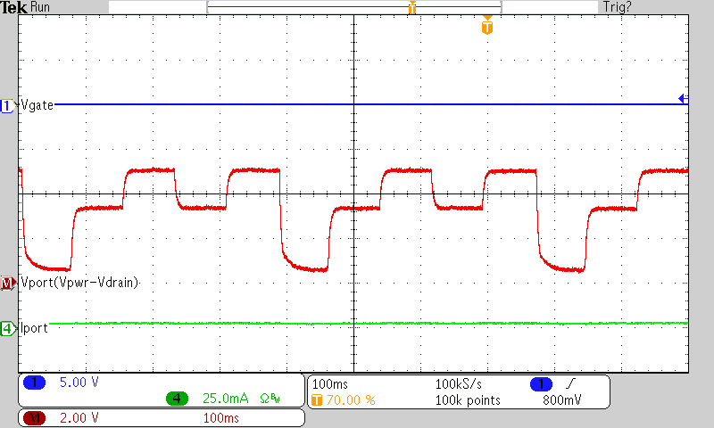
Figure 74. Detection With Invalid PD (15 kΩ and 0.1 μF)
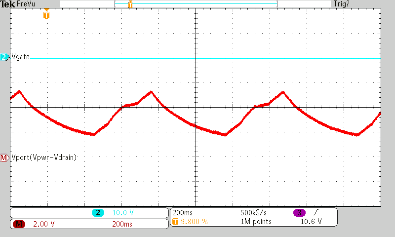
TPS2388 typ_05_Detection_Invalid_PD_25_kohm_LUSC25.png
Figure 76. Detection With Invalid PD (25 kΩ and 10 μF)
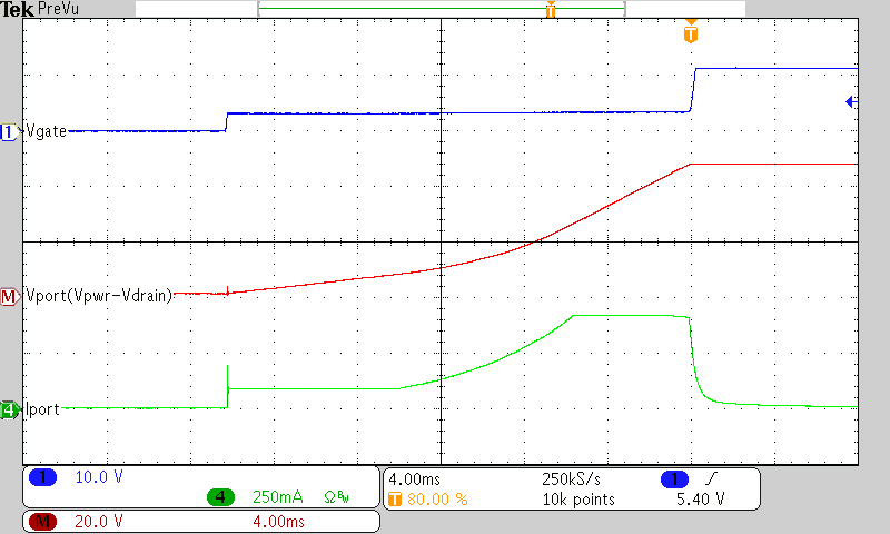
TPS2388 typ_07_Powering_Up_100_microF_Load_LUSC25.png
Figure 78. Powering Up into a 100-μF Load
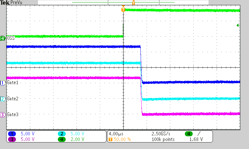
TPS2388 typ_09_All_Ports_Fast_Shutdown_OSS_Input_LUSC25.png
Figure 80. All Ports Fast Shutdown from OSS Input
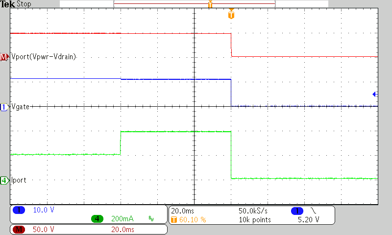
TPS2388 typ_11_Overcurrent_ICUT_Timeout_LUSC25.png
Figure 82. Overcurrent (ICUT) Timeout
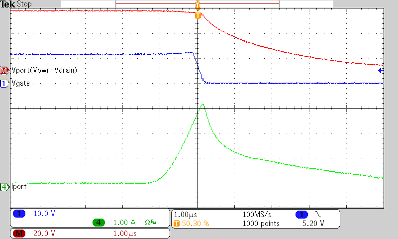
TPS2388 typ_13_Rapid_Response_1_ohm_Short_PoE_LUSC25.png
Figure 84. Rapid Response to a 1-Ω Short - PoE+ Mode
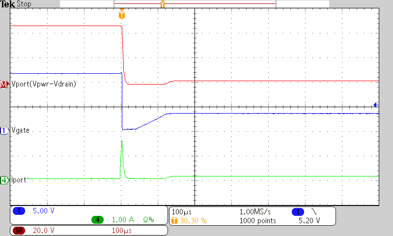
TPS2388 typ_15_Response_25_ohm_Load_PoE_LUSC25.png
Figure 86. Response to a 25-Ω Load - PoE+ Mode
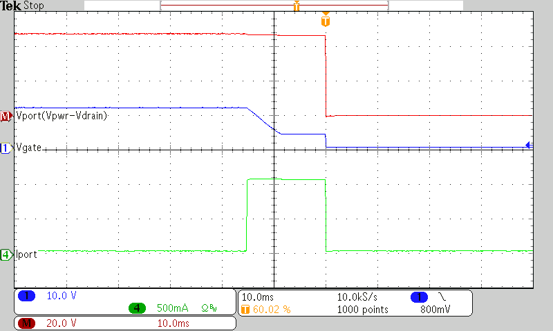
TPS2388 typ_17_Current_Limit_15_ms_Timeout_PoE_45_ohm_Load_LUSC25.png
Figure 88. Current Limit 15-ms Timeout - PoE+ Mode, 45-Ω Load
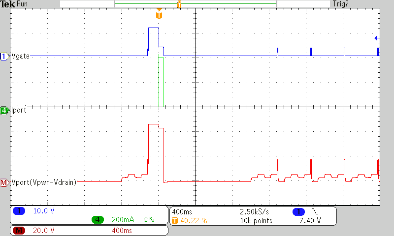
TPS2388 typ_19_Current_Limit_Timeout_Restart_Delay_LUSC25.png
Figure 90. Current Limit Timeout Restart Delay
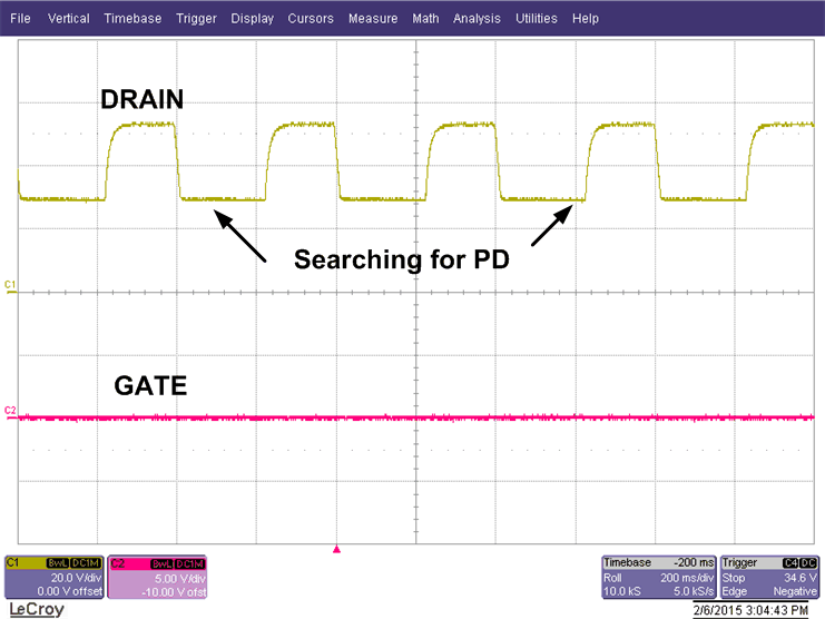
TPS2388 app_01_LUSC24.gifFigure 92. Detection With Open Circuit
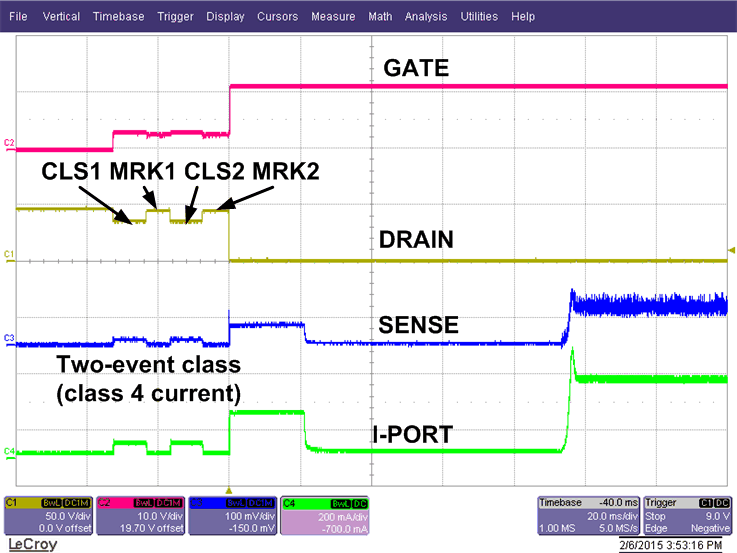
TPS2388 app_03_LUSC24.gifFigure 94. 2-Event Class and Port Turn On
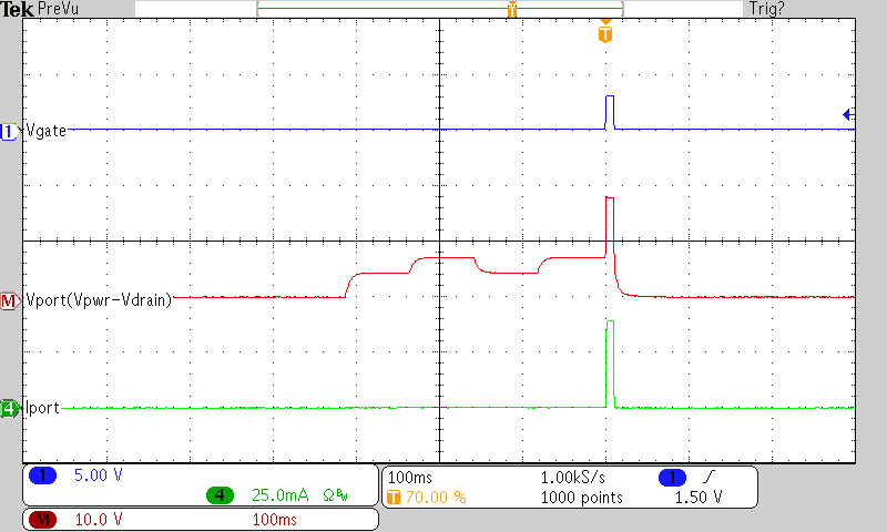
TPS2388 typ_02_Startup_Valid_PD_CLASS_3_LUSC25.png
Figure 73. Startup With Valid PD (25 kΩ and 0.1 μF), Class 3
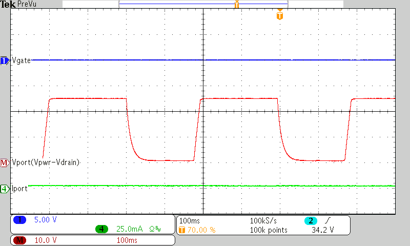
TPS2388 typ_04_Detection_Invalid_PD_open_cir_LUSC25.png
Figure 75. Detection With Invalid PD (Open Circuit)
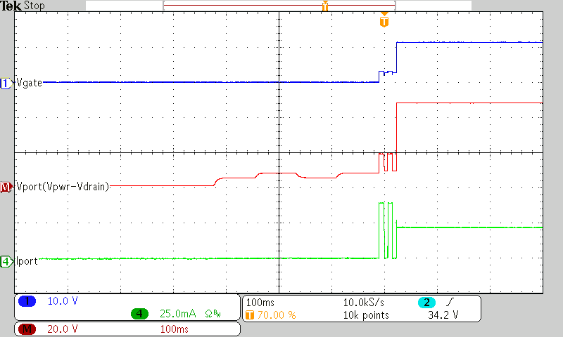
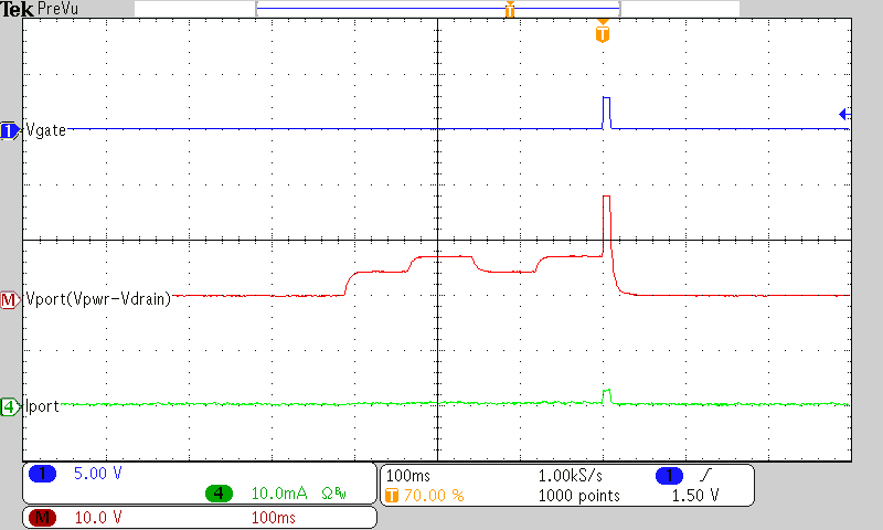
TPS2388 typ_06_2_Event_Class_Startup_Valid_PD_LUSC25.png
Figure 77. 2-Event Class and Startup With Valid PD
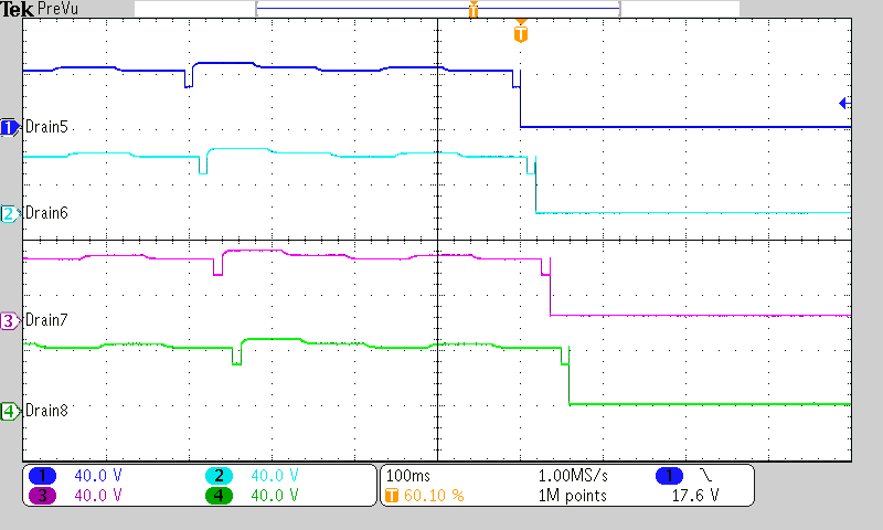
TPS2388 typ_08_All_Ports_Power_On_TPON_Bit_Set_LUSC25.png
Figure 79. All Ports Power-On With TPON Bit Set
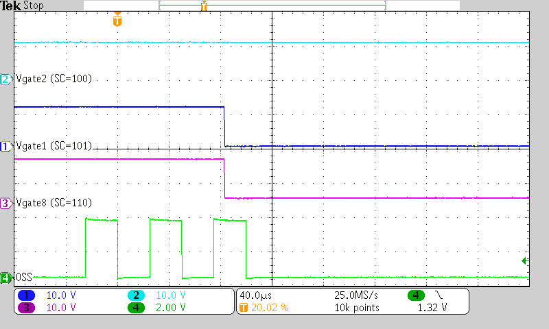
TPS2388 typ_10_Ports_Fast_Shutdown_3_bit_OSS_Input_LUSC25.png
Figure 81. Ports Fast Shutdown from 3-Bit OSS Input
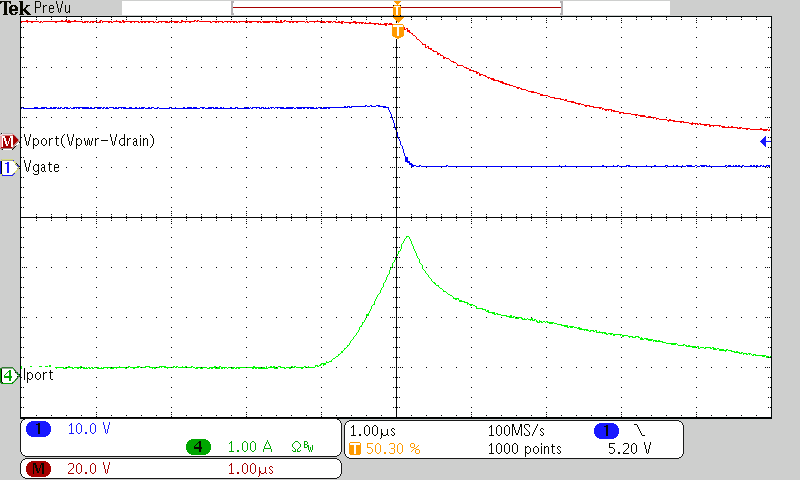
TPS2388 typ_12_Rapid_Response_1_ohm_Short_802.3af_LUSC25.png
Figure 83. Rapid Response to a 1-Ω Short - 802.3af Mode
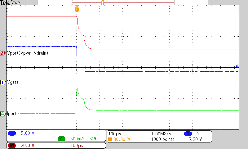
TPS2388 typ_14_Response_50_ohm_Load_802.3af_LUSC25.png
Figure 85. Response to a 50-Ω Load - 802.3af Mode
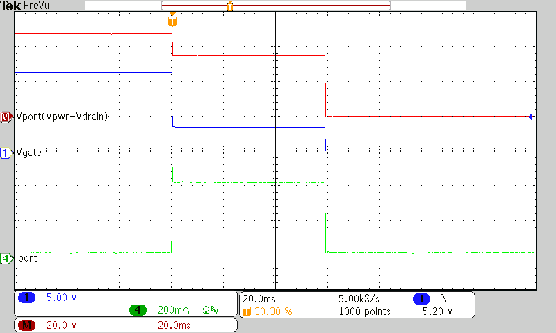
TPS2388 typ_16_Current_Limit_Timeout_802.3af_85_ohm_LUSC25.png
Figure 87. Current Limit Timeout - 802.3af Mode, 85-Ω Load
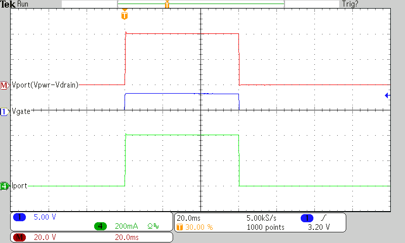
TPS2388 typ_18_Inrush_Fault_Timeout_100_ohm_Load_LUSC25.png
Figure 89. Inrush Fault Timeout - 100-Ω Load
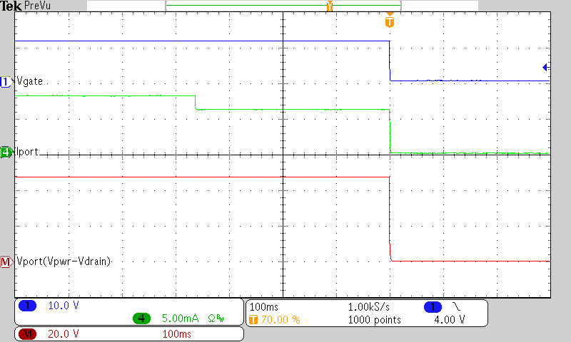
TPS2388 typ_20_Response_to_8_to_6_mA_Load_DC_Disconnect_LUSC25.png
Figure 91. Response to 8-mA to 6-mA Load, DC Disconnect Enabled
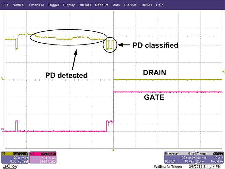
TPS2388 app_02_LUSC24.gifFigure 93. Detection, 2-Event Class and Port Turn On
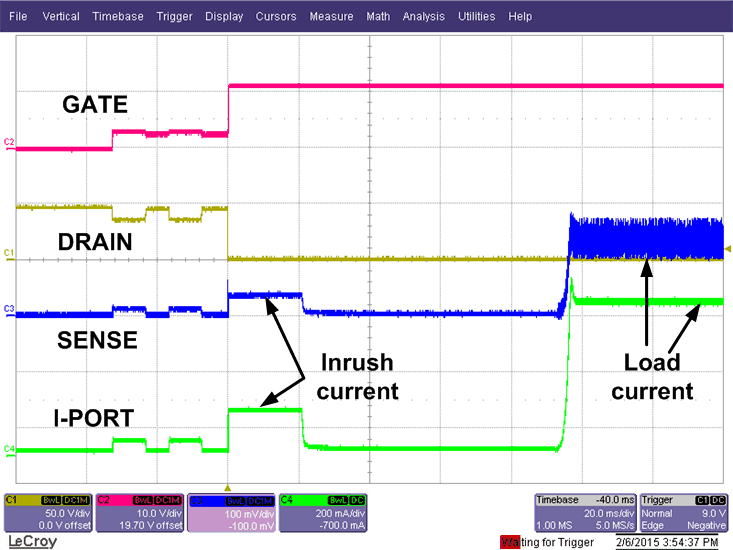
TPS2388 app_04_LUSC24.gifFigure 95. 2-Event Class and Port Turn On