SLUSC25A February 2015 – August 2017 TPS2388
PRODUCTION DATA.
- 1 Features
- 2 Applications
- 3 Description
- 4 Revision History
- 5 Pin Configuration and Functions
- 6 Specifications
- 7 Parameter Measurement Information
-
8 Detailed Description
- 8.1 Overview
- 8.2 Functional Block Diagram
- 8.3 Feature Description
- 8.4 Device Functional Modes
- 8.5 Programming
- 8.6
Register Maps
- 8.6.1 Complete Register Set
- 8.6.2 INTERRUPT Register
- 8.6.3 INTERRUPT MASK Register
- 8.6.4 POWER EVENT Register
- 8.6.5 DETECTION EVENT Register
- 8.6.6 FAULT EVENT Register
- 8.6.7 START/ILIM EVENT Register
- 8.6.8 SUPPLY EVENT Register
- 8.6.9 PORT 1 STATUS Register
- 8.6.10 PORT 2 STATUS Register
- 8.6.11 PORT 3 STATUS Register
- 8.6.12 PORT 4 STATUS Register
- 8.6.13 POWER STATUS Register
- 8.6.14 Pin Status Register
- 8.6.15 OPERATING MODE Register
- 8.6.16 DISCONNECT ENABLE Register
- 8.6.17 DETECT/CLASS ENABLE Register
- 8.6.18 Port Power Priority/ICUT Disable Register Name
- 8.6.19 TIMING CONFIGURATION Register
- 8.6.20 GENERAL MASK Register
- 8.6.21 DETECT/CLASS RESTART Register
- 8.6.22 POWER ENABLE Register
- 8.6.23 RESET Register
- 8.6.24 ID Register
- 8.6.25 Police 21 Configuration Register
- 8.6.26 Police 43 Configuration Register
- 8.6.27 IEEE Power Enable Register
- 8.6.28 Power-on Fault Register
- 8.6.29 PORT RE-MAPPING Register
- 8.6.30 Port 21 Multi Bit Priority Register
- 8.6.31 Port 43 Multi Bit Priority Register
- 8.6.32 TEMPERATURE Register
- 8.6.33 INPUT VOLTAGE Register
- 8.6.34 PORT 1 CURRENT Register
- 8.6.35 PORT 2 CURRENT Register
- 8.6.36 PORT 3 CURRENT Register
- 8.6.37 PORT 4 CURRENT Register
- 8.6.38 PORT 1 VOLTAGE Register
- 8.6.39 PORT 2 VOLTAGE Register
- 8.6.40 PORT 3 VOLTAGE Register
- 8.6.41 PORT 4 VOLTAGE Register
- 8.6.42 PoE Plus Register
- 8.6.43 FIRMWARE REVISION
- 8.6.44 I2C WATCHDOG Register
- 8.6.45 DEVICE ID Register
- 8.6.46 PORT 1 DETECT RESISTANCE Register
- 8.6.47 PORT 2 DETECT RESISTANCE Register
- 8.6.48 PORT 3 DETECT RESISTANCE Register
- 8.6.49 PORT 4 DETECT RESISTANCE Register
- 9 Application and Implementation
- 10Power Supply Recommendations
- 11Layout
- 12Device and Documentation Support
- 13Mechanical, Packaging, and Orderable Information
パッケージ・オプション
メカニカル・データ(パッケージ|ピン)
- RTQ|56
サーマルパッド・メカニカル・データ
- RTQ|56
発注情報
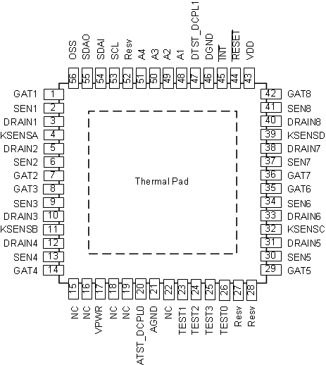
5 Pin Configuration and Functions
RTQ Package
VQFN 56 Pins
Top View

Pin Functions
| PIN | I/O | DESCRIPTION | |
|---|---|---|---|
| NAME | NO. | ||
| A1-4 | 48–51 | I | I2C A1-A4 address lines. These pins are internally pulled up to VDD. |
| AGND | 21 | — | Analog ground. Connect to GND plane and exposed thermal pad. |
| ATST_DCPL0 | 20 | O | Used for internal test purposes, no bypass capacitor is needed. |
| DGND | 46 | — | Digital ground. Connect to GND plane and exposed thermal pad. |
| DRAIN1-8 | 3, 5, 10, 12, 31, 33, 38, 40 | I | Port 1-8 output voltage monitor. |
| DTST_DCPL1 | 47 | O | Used for internal test purposes, no bypass capacitor is needed. |
| GAT1-8 | 1, 7, 8, 14, 29, 35, 36, 42 | O | Port 1-8 gate drive output. |
| INT | 45 | O | Interrupt output. This pin asserts low when a bit in the interrupt register is asserted. This output is open-drain. |
| KSENSA/B | 4, 11 | I | Kelvin point connection for SEN1-4 |
| KSENSC/D | 32, 39 | I | Kelvin point connection for SEN5-8 |
| NC | 15, 16, 18, 19 | O | No connect pins. These pins are internally biased at 1/3 and 2/3 of VPWR in order to control the voltage gradient from VPWR. Leave open. |
| 22 | — | No connect pin. Leave open. | |
| OSS | 56 | I | Port 1-8 fast shutdown. This pin is internally pulled down to DGND. |
| Thermal pad | — | — | The DGND and AGND terminals must be connected to the exposed thermal pad for proper operation. |
| RESET | 44 | I | Reset input. When asserted low, the TPS2388 is reset. This pin is internally pulled up to VDD. |
| Resv | 27, 28, 52 | — | Reserved. No connect pins. Leave open. |
| SCL | 53 | I | Serial clock input for I2C bus. |
| SDAI | 54 | I | Serial data input for I2C bus. This pin can be connected to SDAO for non-isolated systems. |
| SDAO | 55 | O | Serial data output for I2C bus. This pin can be connected to SDAI for non-isolated systems. This output is open-drain. |
| SEN1-8 | 2, 6, 9, 13, 30, 34, 37, 41 | I | Port 1-8 current sense input. |
| TEST0-3 | 23, 24, 25, 26 | I/O | Used internally for test purposes only. Leave open. |
| VDD | 43 | — | Digital supply. Bypass with 0.1 µF to DGND pin. |
| VPWR | 17 | — | Analog 48-V positive supply. Bypass with 0.1 µF to AGND pin. |