JAJSCH5 September   2016 TPS2552D , TPS2553D

PRODUCTION DATA.  

  1. 特長
  2. アプリケーション
  3. 概要
  4. 改訂履歴
  5. Device Comparison Table
  6. Pin Configuration and Functions
  7. Specifications
    1. 7.1 Absolute Maximum Ratings
    2. 7.2 ESD Ratings
    3. 7.3 Recommended Operating Conditions
    4. 7.4 Thermal Information
    5. 7.5 Electrical Characteristics
    6. 7.6 Typical Characteristics
  8. Parameter Measurement Information
  9. Detailed Description
    1. 9.1 Overview
    2. 9.2 Functional Block Diagram
    3. 9.3 Feature Description
      1. 9.3.1 Overcurrent Conditions
      2. 9.3.2 Reverse-Voltage Protection
      3. 9.3.3 FAULT Response
      4. 9.3.4 Undervoltage Lockout (UVLO)
      5. 9.3.5 ENABLE
      6. 9.3.6 Thermal Sense
    4. 9.4 Device Functional Modes
    5. 9.5 Programming
      1. 9.5.1 Programming the Current-Limit Threshold
  10. 10Application and Implementation
    1. 10.1 Application Information
      1. 10.1.1 Constant-Current and Impact on Output Voltage
    2. 10.2 Typical Applications
      1. 10.2.1 Two-Level Current-Limit Circuit
        1. 10.2.1.1 Design Requirements
        2. 10.2.1.2 Detailed Design Procedures
          1. 10.2.1.2.1 Designing Above a Minimum Current Limit
          2. 10.2.1.2.2 Designing Below a Maximum Current Limit
          3. 10.2.1.2.3 Accounting for Resistor Tolerance
          4. 10.2.1.2.4 Input and Output Capacitance
        3. 10.2.1.3 Application Curves
      2. 10.2.2 Auto-Retry Functionality
        1. 10.2.2.1 Design Requirements
        2. 10.2.2.2 Detailed Design Procedure
      3. 10.2.3 Typical Application as USB Power Switch
        1. 10.2.3.1 Design Requirements
          1. 10.2.3.1.1 USB Power-Distribution Requirements
        2. 10.2.3.2 Detailed Design Procedure
          1. 10.2.3.2.1 Universal Serial Bus (USB) Power-Distribution Requirements
  11. 11Power Supply Recommendations
    1. 11.1 Self-Powered and Bus-Powered Hubs
    2. 11.2 Low-Power Bus-Powered and High-Power Bus-Powered Functions
    3. 11.3 Power Dissipation and Junction Temperature
  12. 12Layout
    1. 12.1 Layout Guidelines
    2. 12.2 Layout Example
  13. 13デバイスおよびドキュメントのサポート
    1. 13.1 デバイス・サポート
    2. 13.2 関連リンク
    3. 13.3 ドキュメントの更新通知を受け取る方法
    4. 13.4 コミュニティ・リソース
    5. 13.5 商標
    6. 13.6 静電気放電に関する注意事項
    7. 13.7 Glossary
  14. 14メカニカル、パッケージ、および注文情報

パッケージ・オプション

メカニカル・データ(パッケージ|ピン)
サーマルパッド・メカニカル・データ
発注情報

12 Layout

12.1 Layout Guidelines

  • TI recommends placing the 100-nF bypass capacitor near the IN and GND pins, and make the connections using a low-inductance trace.
  • TI recommends placing a high-value electrolytic capacitor and a 100-nF bypass capacitor on the output pin is recommended when large transient currents are expected on the output.
  • The traces routing the RILIM resistor to the device should be as short as possible to reduce parasitic effects on the current limit accuracy.
  • The PowerPAD should be directly connected to PCB ground plane using wide and short copper trace.

12.2 Layout Example
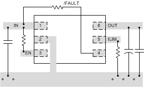
TPS2552D TPS2553D layout_slvs841.gif Figure 30. Layout Recommendation