SLVSDG8B April 2016 – June 2017 TPS25740 , TPS25740A
PRODUCTION DATA.
- 1 Features
- 2 Applications
- 3 Description
- 4 Revision History
- 5 Device Comparison Table
- 6 Pin Configuration and Functions
- 7 Specifications
-
8 Detailed Description
- 8.1 Overview
- 8.2 Functional Block Diagram
- 8.3
Feature Description
- 8.3.1 USB Type-C CC Logic (CC1, CC2)
- 8.3.2 USB PD BMC Transmission (CC1, CC2, VTX)
- 8.3.3 USB PD BMC Reception (CC1, CC2)
- 8.3.4 Discharging (DSCG, VPWR)
- 8.3.5 Configuring Voltage Capabilities (HIPWR, EN9V, EN12V)
- 8.3.6 Configuring Power Capabilities (PSEL, PCTRL, HIPWR)
- 8.3.7 Gate Driver (GDNG, GDNS)
- 8.3.8 Fault Monitoring and Protection
- 8.3.9 Voltage Control (CTL1, CTL2)
- 8.3.10 Sink Attachment Indicator (UFP, DVDD)
- 8.3.11 Power Supplies (VAUX, VDD, VPWR, DVDD)
- 8.3.12 Grounds (AGND, GND)
- 8.3.13 Output Power Supply (DVDD)
- 8.4 Device Functional Modes
-
9 Application and Implementation
- 9.1
Application Information
- 9.1.1 System-Level ESD Protection
- 9.1.2 Use of GD Internal Clamp
- 9.1.3 Resistor Divider on GD for Programmable Start Up
- 9.1.4 Selection of the CTL1 and CTL2 Resistors (R(FBL1) and R(FBL2))
- 9.1.5 Voltage Transition Requirements
- 9.1.6 VBUS Slew Control using GDNG C(SLEW)
- 9.1.7 Tuning OCP Using RF and CF
- 9.2 Typical Application , A/C Power Source (Wall Adapter)
- 9.3 System Examples
- 9.1
Application Information
- 10Power Supply Recommendations
- 11Layout
- 12Device and Documentation Support
- 13Mechanical, Packaging, and Orderable Information
パッケージ・オプション
メカニカル・データ(パッケージ|ピン)
- RGE|24
サーマルパッド・メカニカル・データ
- RGE|24
発注情報
8 Detailed Description
8.1 Overview
The TPS25740 or TPS25740A and supporting circuits perform the functions required to implement a USB Power Delivery (PD) 2.0 as a provider-only and a USB Type-C revision 1.2 source. It uses its CC pins to detect the attachment of a sinking device or upward facing port (UFP) and to determine which of CC1 or CC2 is connected to the CC wire of the cable. It then communicates over the CC wire in the cable bundle using USB PD to offer a set of voltages and currents. USB PD is a technology that utilizes the ubiquitous USB communications and hardware infrastructure to extend the amount of power available to devices from the 7.5 W range for USB BC1.2 to as high as 100 W in a dock. It is a compatible overlay to USB 2.0 and USB 3.0, coexisting with the existing 5 V powered universe of devices by use of adapter cables. Some basic characteristics of this technology relevant to the device include:
- Increased power achieved by providing higher current and/or higher voltage.
- New 3 A cable and 5 A connector to support greater than the traditional 1.5 A.
- Cables have controlled voltage drop
- Voltages greater than 5 V are negotiated between PD partners.
- Standard 5 V is always the default source voltage.
- Voltage and current provisions are negotiated between PD partners.
- PD partners negotiate over the CC line to avoid conflict with existing signaling (that is, D+, D-)
- Layered communication protocol defined including PHY, Protocol Layer, Policy Engine, and Device Policy Manager all implemented within the device.
- The Type-C connector standard implements pre-powerup signaling to determine:
- Connector orientation
- Source 5-V capability
- Detect through connection of a UFP (upward facing port) to a DFP (downward facing port).
- Detection of when the connected UFP is disconnected. VBUS is unpowered until a through-connection is present
Figure 19 and Figure 20 show a typical configuration for the device.
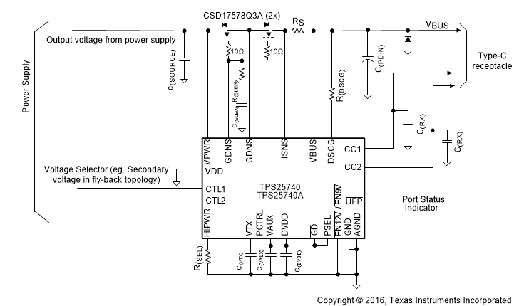 Figure 19. Schematic 1
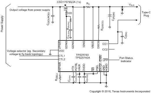 Figure 20. Schematic 2
8.1.1 VBUS Capacitance
The USB Type-C specification requires that the capacitance on the VBUS pin of an empty receptacle be below 10 µF. This is to protect legacy USB sources that are not designed to handle the larger inrush capacitance and which may be connected via an A-to-C cable. For applications with USB Type-C receptacles and large bulk capacitance, this means back-to-back blocking FETs are required as shown in Figure 19. However, for applications with a USB Type-C plug (that is, a captive cable) this requirement does not apply since an adaptor cable with a USB Type-C receptacle and a Type-A plug is not defined or allowed by the USB I/F. Figure 20 is a schematic for such applications.
8.1.2 USB Data Communications
The USB Power Delivery specification requires that sources such as the device advertise in the source capabilities messages they transmit whether or not they are in a product that supports USB data communications. The device is designed for systems without data communication, so it has this bit hard-coded to 0.
8.2 Functional Block Diagram
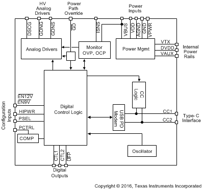
8.3 Feature Description
This section describes the features associated with each pin for the TPS25740 and TPS25740A.
8.3.1 USB Type-C CC Logic (CC1, CC2)
The device uses a current source to implement the pull up resistance USB Type-C requires for Sources. While waiting for a valid connection, the device applies a default pullup of I(RPSTD). A sink attachment is detected when the voltage on one (not both) of the CC pins remains between V(RDSTD) and V(DSTD) for tCcDeb and the voltage on the VBUS pin is below V(VBUS_FTH). Then after turning on VBUS and disabling the Rp current source for the CCx pin not connected through the cable, the device applies I(RP3.0) to advertise 3 A to non-PD sinks. Finally, if it is determined that the attached sink is PD-capable, the device applies I(RP1.5). During this sequence if the voltage on the monitored CC pin exceeds the detach threshold then the device removes VBUS and begins watching for a sink attachment again.
The TPS25740 or TPS25740A digital logic selects the current source switch as illustrated in Figure 21. The schematic shown is replicated for each CC pin.
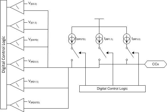 Figure 21. USB Type-C Rp Current Sources and Detection Comparators
If the voltage on both CC pins remains above V(RDSTD) for tCcDeb, then the TPS25740 or TPS25740A goes to the sleep mode. In the sleep mode a less accurate current source is applied and a less accurate comparator watches for attachment (see V(WAKE), and I(DSDFP)).
8.3.2 USB PD BMC Transmission (CC1, CC2, VTX)
An example of the BMC signal, specifically the end of the preamble and beginning of start-of-packet (SOP) is shown below. There is always an edge at the end of each bit or unit interval, and ones have an edge half way through the unit interval.
 Figure 22. BMC Encoded End of Preamble, Beginning of SOP
While engaging in USB PD communications, the TPS25740 or TPS25740A is applying I(RP1.5) or I(RP3.0), so the CC line has a DC voltage of 0.918 V or 1.68 V, respectively. When the BMC signal is transmitted on the CC line, the transmitter overrides this DC voltage as shown in Figure 23. The transmitter bias rail (VTX) is internally generated and may not be used for any other purpose in the system. The VTX pin is only high while the TPS25740 or TPS25740A is transmitting a USB PD message.
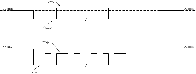 Figure 23. USB PD BMC Transmission on the CC Line
The device transmissions meet the eye diagram USB PD requirements (refer to USB PD in Documentation Support) across the recommended temperature range. Figure 24 shows the transmitter schematic.
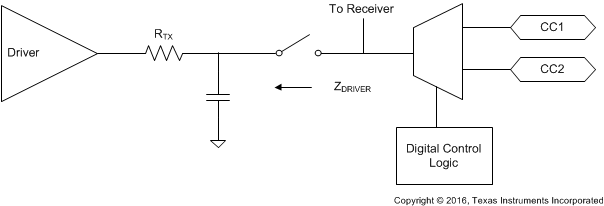 Figure 24. USB PD BMC Transmitter Schematic
The transmit eye diagram shown in Figure 26 was measured using the test load shown in Figure 25 with a CLOAD within the allowed range. The total capacitance CLOAD is computed as:
Where:
- 200 pF < C(RX) < 600 pF
- CCablePlug < 25 pF
- Ca < 625 pF
- 200 pF < CReceiver < 600 pF
Therefore, 400 pF < CLOAD < 1850 pF.
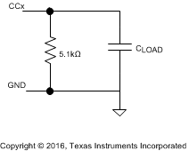 Figure 25. Test Load for BMC Transmitter
Figure 26 shows the transmit eye diagram for the TPS25740 and TPS25740A.
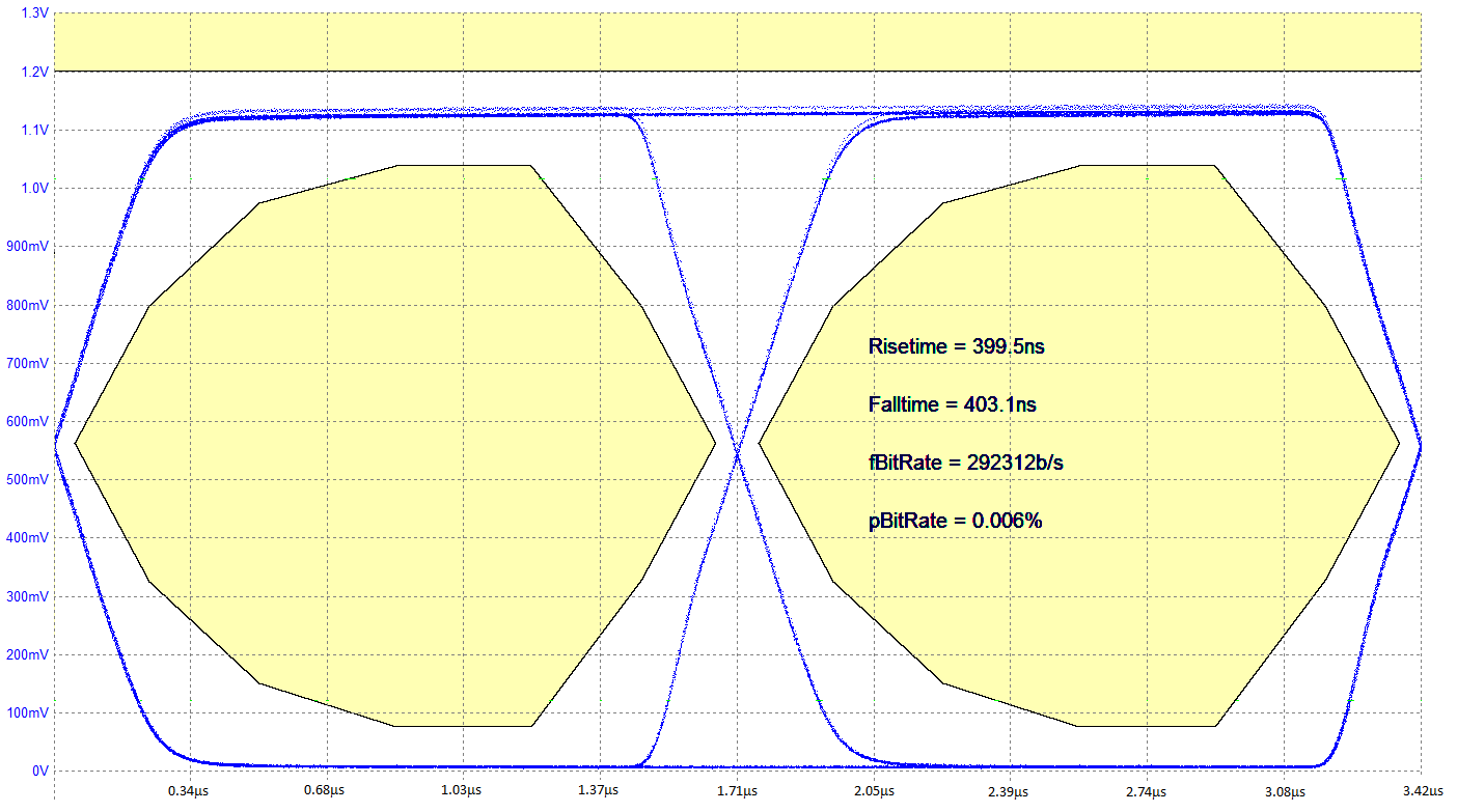 Figure 26. Transmit Eye Diagram (BMC)
8.3.3 USB PD BMC Reception (CC1, CC2)
The TPS25740 or TPS25740A BMC receiver follows the USB PD requirements (refer to USB PD in Documentation Support) using the schematic shown in Figure 27.
The device low-pass filter design and receiver threshold design allows it to reject interference that may couple onto the CC line from a noisy VBUS power supply or any other source (refer to V(INT)).
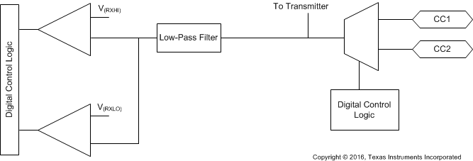 Figure 27. USB PD BMC Receiver Schematic
8.3.4 Discharging (DSCG, VPWR)
The DSCG pin allows for two different pull-downs that are used to apply different discharging strengths. In addition, the VPWR pin is used to apply a load to discharge the power supply bulk capacitance.
If too much power is dissipated by the device (that is, the TJ1 temperature is exceeded) an OTSD occurs that disables the discharge FET; therefore, an external resistor is recommended in series with the DSCG pin to absorb most of the dissipated power. The external resistor R(DSCG) should be chosen such that the current sunk by the DSCG pin does not exceed I(DSCGT).
The VPWR pin should always be connected to the supply side (as opposed to the connector side) of the power-path switch (Figure 28 shows one example). This pin is monitored before enabling the GDNG gate driver to apply the voltage to the VBUS pin of the connector.
From sink attachment, and while the device has not finalized a USB PD contract, the device applies R(DSCGB).
Also from sink attachment, and while the device has not finalized a USB PD contract, the device draws I(SUPP) through the VPWR pin even if VDD is above its UVLO. This helps to discharge the power supply source.
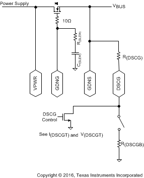 Figure 28. Discharge Schematic
The discharge procedure used in the TPS25740 or TPS25740A is intended to allow the DSCG pin to help pull the power supply down from high voltage, and then also pull VBUS at the connector down to the required level (refer to USB PD in Documentation Support).
8.3.4.1 Discharging after a Fault (VPWR)
There are two types of faults that cause the TPS25740 or TPS25740A to begin a full discharge of VBUS: Slow-shutdown faults and fast-shutdown faults. When a slow-shutdown fault occurs, the device does not disable GDNG until after VBUS is measured below V(SOVP) for a 5V contract. When a fast-shutdown fault occurs, the device disables GDNG immediately and then discharges the connector side of the power-path. In both cases, the bleed discharge is applied to the DSCG pin and I(SUPP) is drawn from the VPWR
Slow-shutdown faults that do not include transmitting a hard reset:
- Receiving a Hard Reset signal (25 ms < tShutdownDelay < 35 ms)
- Cable is unplugged (tShutdownDelay < 20 µs)
Slow-shutdown faults that include transmitting hard reset (25 ms < tShutdownDelay < 35 ms)
- TJ exceeds TJ1 (an overtemperature event)
- Low voltage alarm occurring outside of a voltage transition
- High voltage alarm occurring outside of a voltage transition (but not high enough to cause OVP)
- Receiving an unexpected PD message during a voltage transition
- Failure of power supply to transition voltages within required time of 600 ms (tPSTransition (refer to USB PD in Documentation Support).
- A Soft Reset USB PD message is not acknowledged or Accepted (refer to USB PD in Documentation Support).
- A Request USB PD message is not received in the required time (refer to USB PD in Documentation Support).
- Failure to discharge down to 0.725 V after a fault of any kind.
Fast-shutdown faults (hard reset always sent):
- Fast OVP event occurring at any time.
- OCP event occurring at any time starting from the transmission of the first USB PD message.
- VBUS falling below V(VBUS_FTH) is treated as an OCP event.
- GD falling edge
The DSCG pin is used to discharge the supply line after a slow-shutdown fault occurs. Figure 29 illustrates the signals involved. Depending on the specific slow-shutdown fault the time tShutdownDelay in Figure 29 is different as indicated in the list above. If the slow-shutdown fault triggers a hard reset, it is sent at the beginning of the tShutdownDelay period. However, the device behavior after the time tShutdownDelay is the same for all slow-shutdown faults. After the tShutdownDelay period, the device sets CTL1 and CTL2 to select 5 V from the power supply and puts the DSCG pin into its ON state (Full Discharge). This discharging continues until the voltage on the VBUS pin reaches V(SOVP) for a 5-V contract. The device then disables GDNG and again puts the DSCG pin into its ON state. This discharging state lasts until the voltage on VBUS reaches 0.725 V (nominal). If the discharge does not complete within 650 ms, then the device sends a Hard Reset signal and the process repeats. In Figure 29, the times labeled as t20→5 and t5→0 can vary, they depend on the size of the capacitance to be discharged and the size of the external resistor between the DSCG pin and VBUS. The time labeled as tS is a function of how quickly the NFET opens.
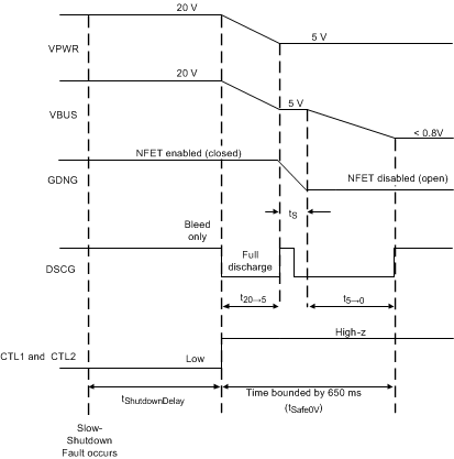 Figure 29. Illustration of Slow-Shutdown VBUS Discharge
Figure 30 illustrates a similar discharge procedure for fast-shutdown faults. The main difference from Figure 29 is that the NFET is opened immediately. It is assumed for the purposes of this illustration that the power supply output capacitance (that is, C(SOURCE) in the reference schematics shown in Figure 19 and Figure 20) is not discharged by the power supply itself, but the VPWR pin is bleeding current from that capacitance. The VPWR pin then draws I(SUPP) after GDNG disables the external NFET. So, as shown in the figure, the VPWR voltage discharges slowly, while the VBUS pin is discharged once the full discharge is enabled. If the voltage on the VPWR pin takes longer than t20→5 + t5→0 + 0.765s to discharge below V(FOVP), then it causes an OVP event and the process repeats.
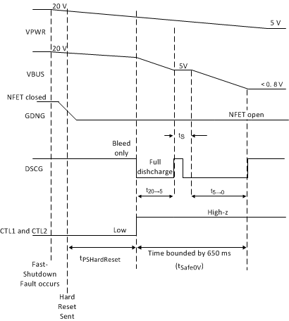 Figure 30. Illustration of Fast-Shutdown Discharge
If the discharge does not complete successfully it is treated as a slow-shutdown fault, and the TPS25740 or TPS25740A repeats the discharge procedure until it does complete successfully. Once the discharge completes successfully as described above (that is, VBUS on connector is below 0.725 V), the device waits for 0.765 s (nominal) before trying to source VBUS again.
8.3.5 Configuring Voltage Capabilities (HIPWR, EN9V, EN12V)
The voltages advertised to USB PD-capable sinks can be configured to one of four different sets. The EN9V, or EN12V pin is not envisioned to be changed dynamically in the system, so changing its state does not trigger sending source capabilities. However, the TPS25740A checks the status of the pin each time before it sends a source capabilities message using USB PD. Note that changing the state of the PCTRL pin forces capabilities to be re-transmitted. The device reads the HIPWR pin after a reset and latches the result.
Table 1. Voltage Programming (TPS25740)
| EN12V PIN | HIPWR PIN | VOLTAGES ADVERTISED via USB PD [V] |
|---|---|---|
| Low | Connected to DVDD or GND directly | 5, 12, 20 |
| Low | Connected to DVDD or GND via R(SEL) | 5, 12 |
| High | Connected to DVDD or GND directly | 5, 20 |
| High | Connected to DVDD or GND via R(SEL) | 5 |
Table 2. Voltage Programming (TPS25740A)
| EN9V PIN | HIPWR PIN | VOLTAGES ADVERTISED via USB PD [V] |
|---|---|---|
| Low | Connected to DVDD or GND directly | 5, 9, 15 |
| Low | Connected to DVDD or GND via R(SEL) | 5, 9 |
| High | Connected to DVDD or GND directly | 5, 15 |
| High | Connected to DVDD or GND via R(SEL) | 5 |
8.3.6 Configuring Power Capabilities (PSEL, PCTRL, HIPWR)
The power advertised to non-PD Type-C Sinks is always 15 W. However, the TPS25740 or TPS25740A only advertises Type-C default current until it debounces the Sink attachment for tCcDeb and the VBUS voltage has been given tVP to stabilize.
The device does not communicate with the cable to determine its capabilities. Therefore, unless the device is in a system with a captive cable able to support 5 A, the HIPWR pin should be used to limit the advertised current to 3 A.
PCTRL is an input pin used to control how much of the maximum allowed power the port will advertise. This pin may be changed dynamically in the system and the device automatically updates any existing USB PD contract. If the PCTRL pin is pulled below V(PCTRL_TH), then the source capabilities offers half of the maximum power specified by the PSEL pin.
The devices read the PSEL and HIPWR pins after a reset and latches the result, but the PCTRL pin is read dynamically by the device and if its state changes new capabilities are calculated and then transmitted.
While USB PD allows advertising a power of 100 W, UL certification for Class 2 power units (UL 1310) requires the maximum power remain below 100 W. The TPS25740 only advertises up to 4.65 A for a 20-V contract, this allows the VBUS overshoot to reach 21.5 V as allowed by USB PD while remaining within the UL certification limits. Therefore, the TPS25740 allows delivering 100 W of power without adding additional voltage tolerance constraints on the power supply.
The PSEL pin offers four possible maximum power settings, but the devices can actually advertise more power settings depending upon the state of the HIPWR and PCTRL pins. Table 3 summarizes the four maximum power settings that are available via PSEL, again note this is not necessarily the maximum power that is advertised.
Table 3. PSEL Configurations
| Maximum Power (PSEL) [W] |
PSEL |
|---|---|
| P(SEL) = 36 | Direct to GND |
| P(SEL) = 45 | DVDD via R(SEL) |
| P(SEL)= 65 | GND via R(SEL) |
| P(SEL) = 93 | Direct to DVDD |
Equation 2 provides a quick reference which applies to both TPS25740 and TPS25740A to see how the HIPWR, PSEL and PCTRL pins affect what current is advertised with each voltage in the source capabilities message:

Where:
- For a voltage Vx, the advertised current is Ix
- If the PCTRL pin is low, then Pmax = P(SEL) / 2
- If the PCTRL pin is high, then Pmax = P(SEL).
- If the HIPWR pin is pulled high, then Imax = 3 A.
- If the HIPWR pin is pulled low, then Imax = 5 A.
Table 4 and Table 5 provide a comprehensive list of the currents and voltages that are advertised for each voltage.
Table 4. Maximum Current Advertised in the Power Data Object for a Given Voltage (TPS25740)
| PSEL | VOLTAGE [V] | HIPWR | MAXIMUM CURRENT PCTRL = LOW [A] |
MAXIMUM CURRENT PCTRL = HIGH [A] |
|---|---|---|---|---|
| Direct to GND | 5 | Max = 3 A DVDD through R(SEL) or Direct to DVDD |
3 | 3 |
| DVDD via R(SEL) | 3 | 3 | ||
| GND via R(SEL) | 3 | 3 | ||
| Direct to DVDD | 3 | 3 | ||
| Direct to GND | 12 | 1.5 | 3 | |
| DVDD via R(SEL) | 1.87 | 3 | ||
| GND via R(SEL) | 2.7 | 3 | ||
| Direct to DVDD | 3 | 3 | ||
| Direct to GND | 20 | Max = 3 A Direct to DVDD |
0.9 | 1.8 |
| DVDD via R(SEL) | 1.12 | 2.24 | ||
| GND via R(SEL) | 1.62 | 3 | ||
| Direct to DVDD | 2.32 | 3 | ||
| Direct to GND | 5 | Max = 5 A GND through R(SEL) or Direct to GND |
3.6 | 5 |
| DVDD via R(SEL) | 4.5 | 5 | ||
| GND via R(SEL) | 5 | 5 | ||
| Direct to DVDD | 5 | 5 | ||
| Direct to GND | 12 | 1.5 | 3 | |
| DVDD via R(SEL) | 1.87 | 3.74 | ||
| GND via R(SEL) | 2.7 | 5 | ||
| Direct to DVDD | 4.16 | 5 | ||
| Direct to GND | 20 | Max = 5 A Direct to GND |
0.9 | 1.8 |
| DVDD via R(SEL) | 1.12 | 2.24 | ||
| GND via R(SEL) | 1.62 | 3.24 | ||
| Direct to DVDD | 2.32 | 4.64 |
Table 5. Maximum Current Advertised in the Power Data Object for a Given Voltage (TPS25740A)
| PSEL | VOLTAGE [V] | HIPWR | MAXIMUM CURRENT PCTRL = LOW [A] |
MAXIMUM CURRENT PCTRL = HIGH [A] |
|---|---|---|---|---|
| Direct to GND | 5 | Max = 3 A DVDD through R(SEL) or Direct to DVDD |
3 | 3 |
| DVDD via R(SEL) | 3 | 3 | ||
| GND via R(SEL) | 3 | 3 | ||
| Direct to DVDD | 3 | 3 | ||
| Direct to GND | 9 | 2 | 3 | |
| DVDD via R(SEL) | 2.5 | 3 | ||
| GND via R(SEL) | 3 | 3 | ||
| Direct to DVDD | 3 | 3 | ||
| Direct to GND | 15 | Max = 3 A Direct to DVDD |
1.2 | 2.4 |
| DVDD via R(SEL) | 1.5 | 3 | ||
| GND viaR(SEL) | 2.17 | 3 | ||
| Direct to DVDD | 3 | 3 | ||
| Direct to GND | 5 | Max = 5 A GND through R(SEL) or Direct to GND |
3.6 | 5 |
| DVDD via R(SEL) | 4.5 | 5 | ||
| GND via R(SEL) | 5 | 5 | ||
| Direct to DVDD | 5 | 5 | ||
| Direct to GND | 9 | 2 | 4 | |
| DVDD via R(SEL) | 2.5 | 5 | ||
| GND via R(SEL) | 3.61 | 5 | ||
| Direct to DVDD | 5 | 5 | ||
| Direct to GND | 15 | Max = 5 A Direct to GND |
1.2 | 2.4 |
| DVDD via R(SEL) | 1.5 | 3 | ||
| GND via R(SEL) | 2.17 | 4.34 | ||
| Direct to DVDD | 3.1 | 5 |
8.3.7 Gate Driver (GDNG, GDNS)
The GDNG and GDNS pins may control a single NFET or back-to-back NFETs in a common-source configuration. The GDNS is used to sense the voltage so that the voltage differential between the pins is maintained.
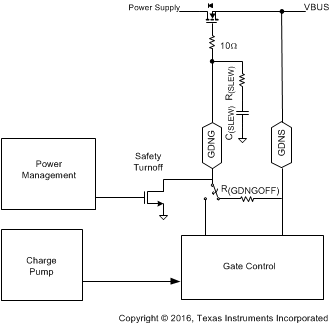 Figure 31. GDNG/GDNS Gate Control
8.3.8 Fault Monitoring and Protection
8.3.8.1 Over/Under Voltage (VBUS)
The TPS25740 or TPS25740A uses the VBUS pin to monitor for overvoltage or undervoltage conditions and implement the fast-OVP, slow-OVP and slow-UVP features.
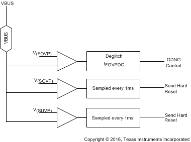 Figure 32. Voltage Monitoring Circuits
If an over-voltage condition is sensed by the Fast OVP mechanism, GDNG is disabled within tFOVP + tFOVPDG, then a Hard Reset is transmitted and the VBUS discharge sequence is started. At power up the voltage trip point is set to V(FOVP) (5 V contract). When a contract is negotiated the trip point is set to the corresponding V(FOVP) value.
The devices employ another slow over-voltage protection mechanism as well that sends the Hard Reset before disabling the external NFET. It catches many OV events before the Fast OVP mechanism. During intentional positive voltage transitions, this mechanism is disabled (see Figure 1). However, tVP after the external NFET has been enabled, if the voltage on the VBUS pin exceeds V(SOVP) then a Hard Reset is transmitted to the Sink and the VBUS discharge sequence is started.
The devices employ a slow under-voltage protection mechanism as well that sends the Hard Reset before disabling GDNG. During intentional negative voltage transitions, this mechanism is disabled (see Figure 1). However, tVP after the external NFET has been enabled if the voltage on the VBUS pin falls below V(SUVP), then a Hard Reset is transmitted to the Sink and the VBUS discharge sequence is started.
8.3.8.2 Over-Current Protection (ISNS, VBUS)
OCP protection is enabled tVP after the voltage on the VBUS pin has exceeded V(VBUS_RTH). Prior to OCP being enabled, the GD pin can be used to protect against a short.
The OCP protection circuit monitors the differential voltage across an external sense resistor to detect when the current outflow exceeds VI(TRIP) which in turn activates an over-current circuit breaker and disables the GDNG / GDNS gate driver. Once the OCP is enabled, if the voltage on the VBUS pin falls below V(VBUS_FTH) then that is also treated like an OCP event.
Following the recommended implementation of a 5-mΩ sense resistor, when the device is configured to deliver 3 A (via HIPWR pin), the OCP threshold lies between 3.8 A and 4.5 A. When configured to deliver 5 A (via HIPWR pin), the OCP threshold lies between 5.8 A and 6.8 A. The resistance of the sense resistor may be tuned to adjust the current that causes VI(TRIP) to be exceeded.
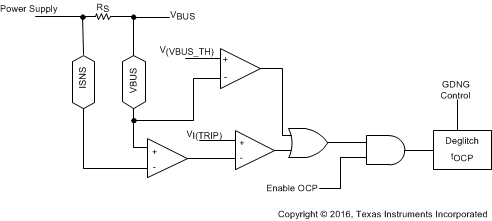 Figure 33. Overcurrent Protection Circuit, (ISNS, VBUS)
8.3.8.3 System Fault Input (GD, VPWR)
The gate-driver disable pin provides a method of overriding the internal control of GDNG and GDNS. A falling edge on GD disables the gate driver within tGDoff. If GD is held low after a sink is attached for 600 ms then a hard reset will be generated and the device sends a hard reset and go through its startup process again.
The GD input can be controlled by a voltage or current source. An internal voltage clamp is provided to limit the input voltage in current source applications. The clamp can safely conduct up to 80 µA and will remain high impedance up to 6.5 V before clamping
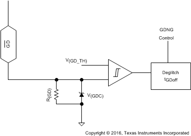 Figure 34. Overcurrent Protection Circuit, (GD)
If the VPWR pin remains below its falling UVLO threshold (V(VPWR_TH)) for more than 600 ms after a sink is attached then the devices consider it a fault and will not enable GDNG. If the VPWR pin is between the rising and falling UVLO threshold, the TPS25740/TPS25740A may enable GDNG and proceed with normal operations. However, after GDNG is enabled, if the VBUS pin does not rise above its UVLO within 190 ms the devices consider it a fast-shutdown fault and disables GDNG. Therefore, in order to ensure USB Type-C compliance and normal operation, the VPWR pin must be above its rising UVLO threshold (V(VPWR_TH)) within 275 ms of when UFP is pulled low and the VBUS pin must be above V(VBUS_RTH) within 190 ms of GDNG being enabled.
8.3.9 Voltage Control (CTL1, CTL2)
CTL1 and CTL2 are open-drain output pins used to control an external power supply as summarized in Table 6. Depending upon the voltage requested by the sink, the device sets the CTL pins accordingly. No current flows into the pin in its high-z state.
Table 6. States of CTL1 and CTL2 as a Function of Target Voltage on VBUS for TPS25740
| VOLTAGE CONTAINED in PDO REQUESTED by UFP | CTL2 STATE | CTL1 STATE |
|---|---|---|
| 5V | High-z | High-z |
| 9 V (TPS25740A) | Low | High-z |
| 12 V (TPS25740) | Low | High-z |
| 15 V (TPS25740A) | Low | Low |
| 20 V (TPS25740) | Low | Low |
8.3.10 Sink Attachment Indicator (UFP, DVDD)
UFP is an open-drain output pin used to indicate the status of the port. It is high-z unless a sink is attached to the port, in which case it is pulled low. A sink attachment is detected when the voltage on one (not both) of the CC pins remains between V(RDSTD) and V(DSTD) for tCcDeb and the voltage on the VBUS pin is below V(VBUS_FTH). After being pulled low, UFP remains low until the sink has been removed for tCcDeb.
DVDD is a power supply pin that is high-z until a sink or debug accessory or audio accessory is attached, in which case it is pulled high. Therefore, it can be used as a sink attachment indicator that is active high.
8.3.11 Power Supplies (VAUX, VDD, VPWR, DVDD)
The VAUX pin is the output of a linear regulator and the input supply for internal power management circuitry. The VAUX regulator draws power from VDD after establishing a USB PD contract unless it is not available in which case it draws from VPWR. Changes in supply voltages will result in seamless switching between supplies.
If there is a load on the DVDD pin, that current will be drawn from the VPWR pin unless the device has stabilized into a USB PD contract or VPWR is below its UVLO.
The device cannot function properly until VPWR is above its UVLO. However, for improved system efficiency when UFP is high-z, VPWR can be low (the high voltage power supply can be disabled) if VDD is above its UVLO.
Connect VAUX to GND via the recommended bypass capacitor. Do not connect any external load that draws more than I(VAUXEXT). Locate the bypass capacitor close to the pin and provide a low impedance ground connection from the capacitor to the ground plane.
VDD should either be grounded or be fed by a low impedance path and have input bypass capacitance. Locate the bypass capacitors close to the VDD and VPWR pins and provide a low impedance ground connection from the capacitor to the ground plane.
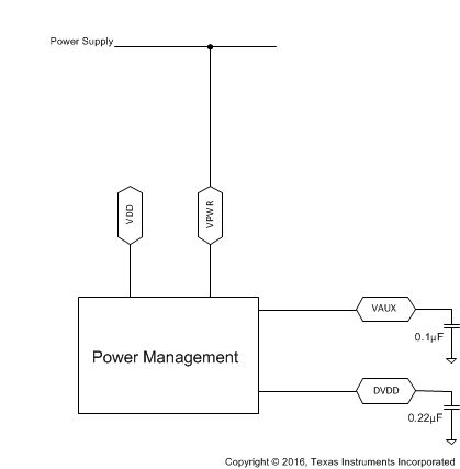 Figure 35. Power Management
8.3.12 Grounds (AGND, GND)
GND is the substrate ground of the die. Most circuits return to GND, but certain analog circuitry returns to AGND to reduce noise and offsets. The power pad (on those devices that possess one) is electrically connected to GND. Connect AGND, GND and the power pad (if present) to the ground plane through the shortest and most direct connections possible.
8.3.13 Output Power Supply (DVDD)
The DVDD pin is the output of an internal 1.85 V linear regulator, and the input supply for internal digital circuitry. This regulator normally draws power from VPWR until a USB PD contract has stabilized, but will seamlessly swap to drawing power from VDD in the event that VPWR drops below its UVLO threshold. External circuitry can draw up to 35 mA from DVDD. Note that as more power is drawn from the DVDD pin more heat is dissipated in the device, and if excessive the OTSD could be tripped which resets the device. Connect DVDD to GND via the recommended ceramic bypass capacitor.
The DVDD pin will only be high when a USB Type-C sink, or audio accessory, or debug accessory is attached, refer to Figure 17 and Figure 18.
Locate the bypass capacitor close to the pin and provide a low impedance ground connection from the capacitor to the ground plane.
8.4 Device Functional Modes
8.4.1 Sleep Mode
Many adaptors that include USB PD must consume low quiescent power to meet regulatory requirements (that is, “Green,” Energy Star, or such). The device supports the sleep mode to minimize power consumption when the receptacle or plug is unattached. The device enters sleep mode when there is no valid plug termination attached; a valid plug termination is defined as one of: sink, Audio accessory, or Debug accessory. If an active cable is attached but its far-end is left unconnected or “dangling,” then the device also enters sleep mode. It exits the sleep mode whenever the plug status changes, that could be a dangling cable being removed or a sink being connected.
8.4.2 Checking VBUS at Start Up
When first powered up, the device will not enable GDNG if the voltage on VBUS is already above its UVLO. This is a protective measure taken to avoid the possibility of turning on while connected to another active power supply in some non-compliant configuration.
This means that the VBUS pin must be connected between the power-path NFET and the USB connector. This also allows for a controlled discharge of VBUS all the way down to the required voltage on the connector (refer to USB PD in Documentation Support).