JAJSDY1C June 2017 – March 2018 TPS25740B
PRODUCTION DATA.
- 1 特長
- 2 アプリケーション
- 3 概要
- 4 改訂履歴
- 5 概要(続き)
- 6 Device Comparison Table
- 7 Pin Configuration and Functions
- 8 Specifications
-
9 Detailed Description
- 9.1 Overview
- 9.2 Functional Block Diagram
- 9.3
Feature Description
- 9.3.1 ENSRC
- 9.3.2 USB Type-C CC Logic (CC1, CC2)
- 9.3.3 USB PD BMC Transmission (CC1, CC2, VTX)
- 9.3.4 USB PD BMC Reception (CC1, CC2)
- 9.3.5 Discharging (DSCG, VPWR)
- 9.3.6 Configuring Voltage Capabilities (HIPWR)
- 9.3.7 Configuring Power Capabilities (PSEL, PCTRL, HIPWR)
- 9.3.8 Gate Driver (GDNG, GDNS)
- 9.3.9 Fault Monitoring and Protection
- 9.3.10 Voltage Control (CTL1, CTL2,CTL3)
- 9.3.11 Sink Attachment Indicator (DVDD)
- 9.3.12 Power Supplies (VAUX, VDD, VPWR, DVDD)
- 9.3.13 Grounds (AGND, GND)
- 9.3.14 Output Power Supply (DVDD)
- 9.4 Device Functional Modes
-
10Application and Implementation
- 10.1
Application Information
- 10.1.1 System-Level ESD Protection
- 10.1.2 Using ENSRC to Enable the Power Supply upon Sink Attachment
- 10.1.3 Use of GD Internal Clamp
- 10.1.4 Resistor Divider on GD for Programmable Start Up
- 10.1.5 Selection of the CTL1, CTL2, and CTL3 Resistors (R(FBL1), R(FBL2), and R(FBL3))
- 10.1.6 Voltage Transition Requirements
- 10.1.7 VBUS Slew Control using GDNG C(SLEW)
- 10.1.8 Tuning OCP using RF and CF
- 10.2 Typical Applications
- 10.3 System Examples
- 10.1
Application Information
- 11Power Supply Recommendations
- 12Layout
- 13デバイスおよびドキュメントのサポート
- 14メカニカル、パッケージ、および注文情報
パッケージ・オプション
メカニカル・データ(パッケージ|ピン)
- RGE|24
サーマルパッド・メカニカル・データ
- RGE|24
発注情報
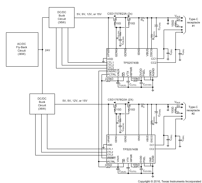
10.3.3 Dual-Port A/C Power Source (Wall Adaptor)
In this system design example, the PSEL pin is configured such that P(SEL) = 36 W, and 5 V, 9 V, 12 V are offered at a maximum of 3 A while 15 V is offered at a maximum of 2.4A. The over-current protection (OCP) trip point is set just above 3 A.
The ENSRC pin from one TPS25740B is attached to the PCTRL pin on the other TPS25740B. When one port is not active (no UFP attached through the receptacle) its ENSRC pin is left high-z so the PCTRL pin on the other port is pulled high. This allows the adaptor to provide up to the full 36 W on a single port if a single UFP is attached. If two UFP’s are attached (one to each port) then each port only offers current that would reach a maximum of 18 W. So each port is allocated half of the overall power when each port has a UFP attached.
 Figure 69. Dual-Port Adapter Provider Concept