-
TPS25925x, TPS25926x Simple 5-V/12-V eFuse Protection Switches
- 1 Features
- 2 Applications
- 3 Description
- 4 Revision History
- 5 Device Comparison Table
- 6 Pin Configuration and Functions
- 7 Specifications
- 8 Detailed Description
-
9 Application and Implementation
- 9.1 Application Information
- 9.2 Typical Application
- 10Power Supply Recommendations
- 11Layout
- 12Device and Documentation Support
- 13Mechanical, Packaging, and Orderable Information
- IMPORTANT NOTICE
パッケージ・オプション
メカニカル・データ(パッケージ|ピン)
- DRC|10
サーマルパッド・メカニカル・データ
- DRC|10
発注情報
TPS25925x, TPS25926x Simple 5-V/12-V eFuse Protection Switches
1 Features
- 12-V eFuse – TPS25926x
- 5-V eFuse – TPS25925x
- Integrated 30-mΩ Pass MOSFET
- Fixed Over-Voltage Clamp:
- 6.1-V Clamp - TPS25925x
- 15-V Clamp - TPS25926x
- 2-A to 5-A Adjustable ILIMIT (±15% Accuracy)
- Programmable VOUT Slew Rate, UVLO
- Built-in Thermal Shutdown
- UL 2367 Recognized – File No. E339631*
- *RILIM ≤ 130 kΩ (5 A maximum)
- Safe During Single Point Failure Test (UL60950)
- Small Foot Print – 10L (3 mm x 3 mm) VSON
2 Applications
- HDD and SSD Drives
- Set Top Boxes
- Servers and AUX Supplies
- PCI and PCIe Cards
- Adapter Powered Devices
3 Description
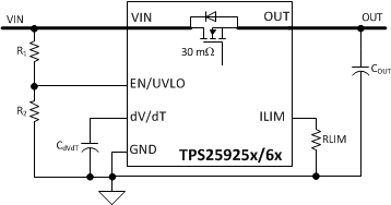
The TPS25925x/6x family of eFuses is a highly integrated circuit protection and power management solution in a tiny package. The devices use few external components and provide multiple protection modes. They are a robust defense against overloads, shorts circuits, voltage surges, excessive inrush current. Current limit level can be set with a single external resistor and current limit set has a typical accuracy of ±15%. Over voltage events are limited by internal clamping circuits to a safe fixed maximum, with no external components required. TPS25926x devices provide over voltage protection (OVP) for 12-V systems and TPS25925x devices for 5-V systems. In cases with particular voltage ramp requirements, a dV/dT pin is provided that can be programmed with a single capacitor to ensure proper output ramp rates.
Device Information(1)
| PART NUMBER | PACKAGE | BODY SIZE (NOM) |
|---|---|---|
| TPS259250, TPS259251 | VSON (10) | 3.00 mm × 3.00 mm |
| TPS259260, TPS259261 |
- For all available packages, see the orderable addendum at the end of the data sheet.
Application Schematic

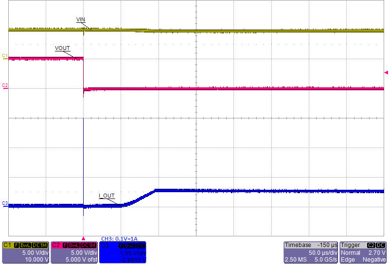
Transient: Output Short Circuit

4 Revision History
Changes from A Revision (August 2015) to B Revision
- Updated Features, Description, Feature Description and Device Functional Modes sectionGo
Changes from * Revision (August 2015) to A Revision
- Changed from Product Preview to Production DataGo
5 Device Comparison Table
| PART NUMBER | UV | OV CLAMP | FAULT RESPONSE | STATUS |
|---|---|---|---|---|
| TPS259250 | 4.3 V | 6.1 V | Latched | Active |
| TPS259251 | 4.3 V | 6.1 V | Auto Retry | Active |
| TPS259260 | 4.3 V | 15 V | Latched | Active |
| TPS259261 | 4.3 V | 15 V | Auto Retry | Active |