JAJSRN4A July   2023  – October 2023 TPS25984

PRODUCTION DATA  

  1.   1
  2. 特長
  3. アプリケーション
  4. 概要
  5. Revision History
  6. 概要 (続き)
  7. Pin Configuration and Functions
  8. Specifications
    1. 7.1 Absolute Maximum Ratings
    2. 7.2 ESD Ratings
    3. 7.3 Recommended Operating Conditions
    4. 7.4 Thermal Information
    5. 7.5 Electrical Characteristics
    6. 7.6 Logic Interface
    7. 7.7 Timing Requirements
    8. 7.8 Switching Characteristics
    9. 7.9 Typical Characteristics
  9. Detailed Description
    1. 8.1 Overview
    2. 8.2 Functional Block Diagram
    3. 8.3 Feature Description
      1. 8.3.1  Undervoltage Protection
      2. 8.3.2  Insertion Delay
      3. 8.3.3  Overvoltage Protection
      4. 8.3.4  Inrush Current, Overcurrent, and Short-Circuit Protection
        1. 8.3.4.1 Slew Rate (dVdt) and Inrush Current Control
          1. 8.3.4.1.1 Start-Up Time Out
        2. 8.3.4.2 Steady-State Overcurrent Protection (Circuit-Breaker)
        3. 8.3.4.3 Active Current Limiting During Start-Up
        4. 8.3.4.4 Short-Circuit Protection
      5. 8.3.5  Analog Load Current Monitor (IMON)
      6. 8.3.6  Mode Selection (MODE)
      7. 8.3.7  Parallel Device Synchronization (SWEN)
      8. 8.3.8  Stacking Multiple eFuses for Unlimited Scalability
        1. 8.3.8.1 Current Balancing During Start-Up
      9. 8.3.9  Analog Junction Temperature Monitor (TEMP)
      10. 8.3.10 Overtemperature Protection
      11. 8.3.11 Fault Response and Indication (FLT)
      12. 8.3.12 Power-Good Indication (PG)
      13. 8.3.13 Output Discharge
      14. 8.3.14 FET Health Monitoring
      15. 8.3.15 Single Point Failure Mitigation
        1. 8.3.15.1 IMON Pin Single Point Failure
        2. 8.3.15.2 ILIM Pin Single Point Failure
        3. 8.3.15.3 IREF Pin Single Point Failure
        4. 8.3.15.4 ITIMER Pin Single Point Failure
    4. 8.4 Device Functional Modes
  10. Application and Implementation
    1. 9.1 Application Information
      1. 9.1.1 Single Device, Standalone Operation
      2. 9.1.2 Multiple Devices, Parallel Connection
      3. 9.1.3 Multiple eFuses, Parallel Connection With PMBus
      4. 9.1.4 Digital Telemetry Using External Microcontroller
    2. 9.2 Typical Application: 12-V, 3.3-kW Power Path Protection in Data Center Servers
      1. 9.2.1 Application
      2. 9.2.2 Design Requirements
      3. 9.2.3 Detailed Design Procedure
      4. 9.2.4 Application Curves
    3. 9.3 Best Design Practices
    4. 9.4 Power Supply Recommendations
      1. 9.4.1 Transient Protection
      2. 9.4.2 Output short-Circuit Measurements
    5. 9.5 Layout
      1. 9.5.1 Layout Guidelines
      2. 9.5.2 Layout Example
  11. 10Device and Documentation Support
    1. 10.1 Documentation Support
      1. 10.1.1 Related Documentation
    2. 10.2 サポート・リソース
    3. 10.3 Trademarks
    4. 10.4 静電気放電に関する注意事項
    5. 10.5 用語集
  12. 11Mechanical, Packaging, and Orderable Information

パッケージ・オプション

メカニカル・データ(パッケージ|ピン)
サーマルパッド・メカニカル・データ

Insertion Delay

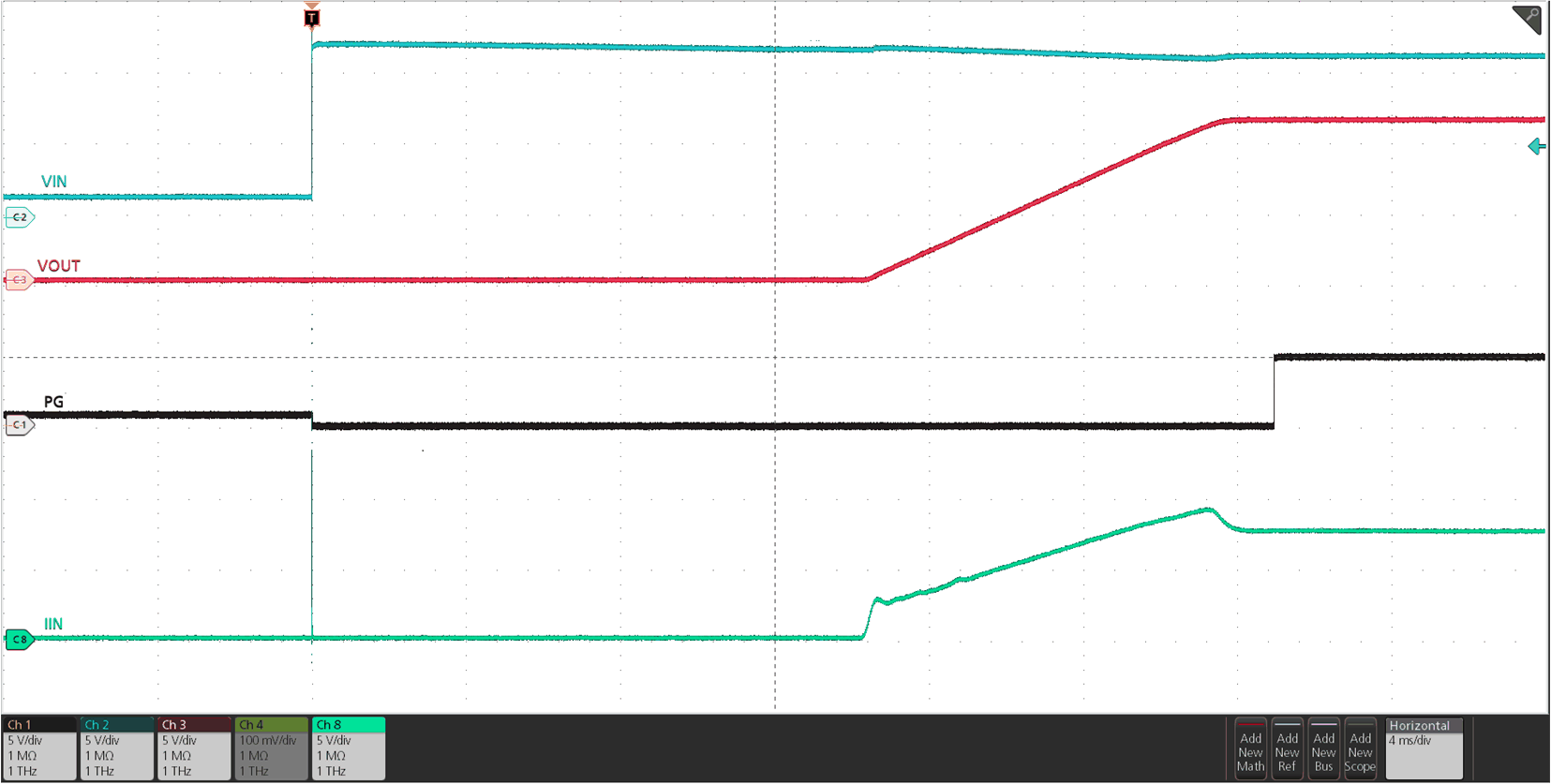
The TPS25984x implements insertion delay at start-up to ensure the supply has stabilized before the device tries to turn on the power to the load. The device initially waits for the VDD supply to rise above the UVP threshold and all the internal bias voltages to settle. After that, the device remains off for an additional delay of tINSDLY irrespective of the EN/UVLO pin condition. This action helps to prevent any unexpected behavior in the system if the device tries to turn on before the card has made firm contact with the backplane or if there is any supply ringing or noise during start-up.
GUID-F5AF4A97-1D1B-4CAE-B235-B2DDC1B9B9B4-low.gif
Input supply stepped up from 0 V to 12 V. Device waits for tINSDLY for input supply to stabilize before it turns on the output.
Figure 8-2 Insertion Delay