SLVSDZ4D February   2018  – February 2020 TPS2HB35-Q1

PRODUCTION DATA.  

  1. Features
  2. Applications
  3. Description
    1.     Simplified Schematic
  4. Revision History
  5. Device Comparison Table
  6. Pin Configuration and Functions
    1.     Pin Functions
    2. 6.1 Recommended Connections for Unused Pins
  7. Specifications
    1. Table 3. Absolute Maximum Ratings
    2. Table 4. ESD Ratings
    3. Table 5. Recommended Operating Conditions
    4. Table 6. Thermal Information
    5. Table 7. Electrical Characteristics
    6. Table 8. SNS Timing Characteristics
    7. Table 9. Switching Characteristics
    8. 7.1      Typical Characteristics
  8. Parameter Measurement Information
  9. Detailed Description
    1. 9.1 Overview
    2. 9.2 Functional Block Diagram
    3. 9.3 Feature Description
      1. 9.3.1 Protection Mechanisms
        1. 9.3.1.1 Thermal Shutdown
        2. 9.3.1.2 Current Limit
          1. 9.3.1.2.1 Current Limit Foldback
          2. 9.3.1.2.2 Programmable Current Limit
          3. 9.3.1.2.3 Undervoltage Lockout (UVLO)
          4. 9.3.1.2.4 VBB During Short-to-Ground
        3. 9.3.1.3 Voltage Transients
          1. 9.3.1.3.1 Load Dump
        4. 9.3.1.4 Driving Inductive Loads
        5. 9.3.1.5 Reverse Battery
        6. 9.3.1.6 Fault Event – Timing Diagrams (Version A/B/C)
      2. 9.3.2 Diagnostic Mechanisms
        1. 9.3.2.1 VOUTx Short-to-Battery and Open-Load
          1. 9.3.2.1.1 Detection With Switch Enabled
          2. 9.3.2.1.2 Detection With Switch Disabled
        2. 9.3.2.2 SNS Output
          1. 9.3.2.2.1 RSNS Value
            1. 9.3.2.2.1.1 High Accuracy Load Current Sense
            2. 9.3.2.2.1.2 SNS Output Filter
        3. 9.3.2.3 Fault Indication and SNS Mux
        4. 9.3.2.4 Resistor Sharing
        5. 9.3.2.5 High-Frequency, Low Duty-Cycle Current Sensing
    4. 9.4 Device Functional Modes
      1. 9.4.1 Off
      2. 9.4.2 Standby
      3. 9.4.3 Diagnostic
      4. 9.4.4 Standby Delay
      5. 9.4.5 Active
      6. 9.4.6 Fault
  10. 10Application and Implementation
    1. 10.1 Application Information
      1. 10.1.1 Ground Protection Network
      2. 10.1.2 Interface With Microcontroller
      3. 10.1.3 I/O Protection
      4. 10.1.4 Inverse Current
      5. 10.1.5 Loss of GND
      6. 10.1.6 Automotive Standards
        1. 10.1.6.1 ISO7637-2
        2. 10.1.6.2 AEC – Q100-012 Short Circuit Reliability
    2. 10.2 Typical Application
      1. 10.2.1 Design Requirements
      2. 10.2.2 Detailed Design Procedure
        1. 10.2.2.1 Thermal Considerations
        2. 10.2.2.2 RILIM Calculation
        3. 10.2.2.3 Diagnostics
          1. 10.2.2.3.1 Selecting the RSNS Value
      3. 10.2.3 Application Curves
  11. 11Power Supply Recommendations
  12. 12Layout
    1. 12.1 Layout Guidelines
    2. 12.2 Layout Example
  13. 13Device and Documentation Support
    1. 13.1 Documentation Support
      1. 13.1.1 Related Documentation
    2. 13.2 Receiving Notification of Documentation Updates
    3. 13.3 Support Resources
    4. 13.4 Trademarks
    5. 13.5 Electrostatic Discharge Caution
    6. 13.6 Glossary
  14. 14Mechanical, Packaging, and Orderable Information

パッケージ・オプション

メカニカル・データ(パッケージ|ピン)
サーマルパッド・メカニカル・データ
発注情報

Table 9. Switching Characteristics

VBB = 13.5 V, TJ = -40°C to +150°C (unless otherwise noted)
PARAMETER TEST CONDITIONS MIN TYP MAX UNIT
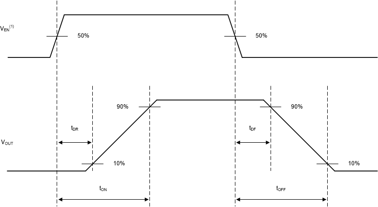
tDR Turnon delay time VBB = 13.5 V, RL ≤ 5 Ω, 50% EN rising to 10% VOUT rising 20 60 100 µs
tDF Turnoff delay time VBB = 13.5 V, RL ≤ 5 Ω, 50% EN falling to 90% VOUT Falling 20 60 100 µs
SRR VOUTx rising slew rate VBB = 13.5 V, 20% to 80% of VOUT,
RL ≤ 5 Ω
0.1 0.4 0.7 V/µs
SRF VOUTx falling slew rate VBB = 13.5 V, 80% to 20% of VOUT,
RL ≤ 5 Ω
0.1 0.4 0.7 V/µs
tON Turnon time VBB = 13.5 V, RL ≤ 5 Ω, 50% EN rising to 80% VOUT rising 39 87 145 µs
tOFF Turnoff time VBB = 13.5 V, RL ≤ 5 Ω, 50% EN rising to 80% VOUT rising 39 87 147 µs
tON - tOFF Turnon and turnoff matching 200-µs enable pulse –50 0 50 µs
EON Switching energy losses during turnon VBB = 13.5 V, RL ≤ 5 Ω 0.6 mJ
EOFF Switching energy losses during turnoff VBB = 13.5 V, RL ≤ 5 Ω 0.6 mJ
TPS2HB35-Q1 switch_char_def_TPS1HBxx.gif
Rise and fall time of VENx is 100 ns.
Figure 1. Switching Characteristics Definitions
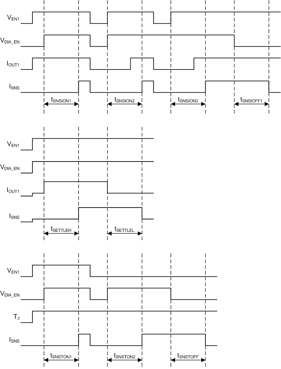
TPS2HB35-Q1 sns_tim_char_def_slvsd84.gif

NOTE1:

Rise and fall times of control signals are 100 ns. Control signals include: EN1, EN2, DIA_EN, SEL1, SEL2.

NOTE2:

SEL1 and SEL2 must be set to the appropriate values.
Figure 2. SNS Timing Characteristics Definitions