SLVS227G August 1999 – June 2024
PRODUCTION DATA
- 1
- 1 Features
- 2 Applications
- 3 Description
- 4 Device Comparison
- 5 Pin Configuration and Functions
- 6 Specifications
- 7 Detailed Description
- 8 Device and Documentation Support
- 9 Revision History
- 10Mechanical, Packaging, and Orderable Information
パッケージ・オプション
デバイスごとのパッケージ図は、PDF版データシートをご参照ください。
メカニカル・データ(パッケージ|ピン)
- DBV|5
サーマルパッド・メカニカル・データ
発注情報
3 Description
The TPS312x family of voltage supervisory circuits provides voltage monitoring down to 1.2V rails and timing supervision, primarily for DSP and processor-based systems. All devices in the family monitor the power rail and assert RESET output when the power rail is under the threshold voltage target (VIT-). The threshold voltage is programmed into the device to minimize external components. Built-in hysteresis prevents false triggering. The RESET output is not valid for supply voltage (VDD) under 0.75V. The TPS312x family includes devices with active high output for use as disable during malfunction and active-low outputs for most systems where high output indicates properly functioning system.
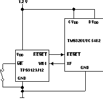
The TPS3123/3124/3128 also include the watchdog timer functionality to monitor timely digital pulses from the processor and issue an alert if the expected pulse does not arrive on time due to potential software freeze or hang. Such integration of supply rail monitoring and the watch dog timer feature is very helpful in always on systems, such as Factory Automation and Communications Infrastructure.
In addition the TPS3123/5/6/8 devices incorporate a manual reset input, MR, to force RESET triggered by an event unrelated to the voltage rail monitoring of the pulses monitored by the watch dog timer. A low level at MR causes RESET to become active. The TPS3124 devices do not have the input MR, but include a high-level output RESET same as the TPS3125 and TPS3126 devices.
All devices in the family are available in a 5-pin SOT23-5 package and are characterized for operation over a temperature range of –40°C to +85°C.
 Typical Low-Voltage DSP Application