JAJSFU0A July   2018  – October 2021 TPS3430

PRODUCTION DATA  

  1. 特長
  2. アプリケーション
  3. 概要
  4. Revision History
  5. Pin Configuration and Functions
  6. Specifications
    1. 6.1 Absolute Maximum Ratings
    2. 6.2 ESD Ratings
    3. 6.3 Recommended Operating Conditions
    4. 6.4 Thermal Information
    5. 6.5 Electrical Characteristics
    6. 6.6 Timing Requirements
    7. 6.7 Timing Diagrams
    8. 6.8 Typical Characteristics
  7. Detailed Description
    1. 7.1 Overview
    2. 7.2 Functional Block Diagrams
    3. 7.3 Feature Description
      1. 7.3.1 CRST
      2. 7.3.2 Window Watchdog
        1. 7.3.2.1 SET0 and SET1
          1. 7.3.2.1.1 Enabling the Window Watchdog
          2. 7.3.2.1.2 Disabling the Watchdog Timer When Using the CRST Capacitor
          3. 7.3.2.1.3 SET0 and SET1 During Normal Watchdog Operation
      3. 7.3.3 Window Watchdog Timer
        1. 7.3.3.1 CWD
        2. 7.3.3.2 WDI Functionality
        3. 7.3.3.3 WDO Functionality
    4. 7.4 Device Functional Modes
      1. 7.4.1 VDD is Below VPOR ( VDD < VPOR)
      2. 7.4.2 VDD is Above VPOR And Below VDD (min)( VPOR < VDD < VDD (min))
      3. 7.4.3 Normal Operation (VDD ≥ VDD (min))
  8. Application and Implementation
    1. 8.1 Application Information
      1. 8.1.1 CRST Delay
        1. 8.1.1.1 Factory-Programmed Watchdog Reset Delay Timing
        2. 8.1.1.2 CRST Programmable Watchdog Reset Delay
      2. 8.1.2 CWD Functionality
        1. 8.1.2.1 Factory-Programmed Timing Options
        2. 8.1.2.2 CWD Adjustable Capacitor Watchdog Timeout
    2. 8.2 Typical Applications
      1. 8.2.1 Monitoring Microcontroller with Watchdog Timer - Design 1
        1. 8.2.1.1 Design Requirements - Design 1
        2. 8.2.1.2 Detailed Design Procedure - Design 1
          1. 8.2.1.2.1 Meeting the Minimum Watchdog Reset Delay - Design 1
          2. 8.2.1.2.2 Setting the Watchdog Window - Design 1
          3. 8.2.1.2.3 Calculating the WDO Pull-up Resistor - Design 1
      2. 8.2.2 Monitoring Microcontroller with a Programmed Window Watchdog Timer - Design 2
        1. 8.2.2.1 Design Requirements - Design 2
        2. 8.2.2.2 Detailed Design Procedure - Design 2
          1. 8.2.2.2.1 Meeting the Minimum Watchdog Reset Delay - Design 2
          2. 8.2.2.2.2 Setting the Watchdog Window - Design 2
          3. 8.2.2.2.3 Calculating the WDO Pull-up Resistor - Design 2
      3. 8.2.3 Monitoring Microcontroller with a Latching Window Watchdog Timer - Design 3
        1. 8.2.3.1 Design Requirements - Design 3
        2. 8.2.3.2 Detailed Design Procedure - Design 3
          1. 8.2.3.2.1 Meeting the Latching Output Requirement - Design 3
          2. 8.2.3.2.2 Setting the Watchdog Window - Design 3
        3. 8.2.3.3 Application Curve - Design 3
  9. Power Supply Recommendations
  10. 10Layout
    1. 10.1 Layout Guidelines
    2. 10.2 Layout Example
  11. 11Device and Documentation Support
    1. 11.1 Device Support
    2. 11.2 Documentation Support
      1. 11.2.1 Related Documentation
    3. 11.3 Receiving Notification of Documentation Updates
    4. 11.4 サポート・リソース
    5. 11.5 Trademarks
    6. 11.6 Electrostatic Discharge Caution
    7. 11.7 Glossary
  12. 12Mechanical, Packaging, and Orderable Information

パッケージ・オプション

メカニカル・データ(パッケージ|ピン)
サーマルパッド・メカニカル・データ
発注情報

Typical Characteristics

all curves are taken at TA = 25°C with 1.6 V ≤ VDD ≤ 6.5 V (unless otherwise noted)
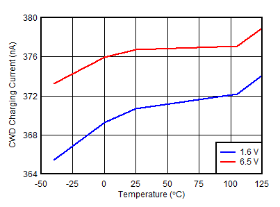
GUID-EFA0A449-83D8-4691-A2B3-CAC6E076F356-low.gifFigure 6-4 CWD Charging Current vs Temperature
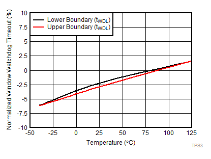
GUID-EFEC8F51-5F18-43D0-A16D-66E7BFEAC604-low.gifFigure 6-6 Normalized Watchdog Timeout Accuracy Over Temperature (SET0 = 1, SET1 = 1, CWD = NC)
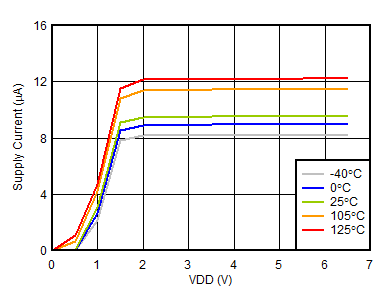
GUID-20B06A0D-B2BA-41F7-A195-33C5FB8C0047-low.gifFigure 6-5 Supply Current vs Power-Supply Voltage
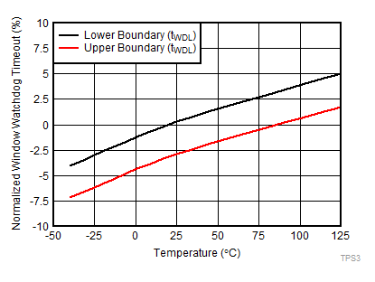
GUID-24646042-5FC5-4BB2-9470-45AB0DAF06F7-low.gifFigure 6-7 Normalized Watchdog Timeout Accuracy Over Temperature (SET0 = 1, SET1 = 1, CWD = 10kΩ to VDD)