SNVSCN2
September 2024
TPS37100-Q1
ADVANCE INFORMATION
1
1
Features
2
Applications
3
Description
4
Device Comparison
5
Pin Configuration and Functions
6
Specifications
6.1
Absolute Maximum Ratings
6.2
ESD Ratings
6.3
Recommended Operating Conditions
6.4
Thermal Information
6.5
Electrical Characteristics
6.6
Switching Characteristics
6.7
Timing Requirements
6.8
Timing Diagrams
6.9
Typical Characteristics
7
Detailed Description
7.1
Overview
7.2
Functional Block Diagram
7.3
Feature Description
7.3.1
Input Voltage (VDD)
7.3.1.1
Undervoltage Lockout (VPOR < VDD < UVLO)
7.3.1.2
Power-On Reset (VDD < VPOR )
7.3.2
SENSE
7.3.2.1
Adjustable Voltage Thresholds
7.3.2.2
SENSE Hysteresis
7.3.2.3
Reverse Polarity Protection
7.3.3
Output Logic Configurations
7.3.3.1
Open-Drain
7.3.3.2
Active-Low (OUT A and OUT B)
7.3.3.3
Latching
7.3.4
User-Programmable Release Time Delay
7.3.4.1
Deassertion Time Delay Configuration
7.3.5
User-Programmable Sense Delay
7.3.5.1
Sense Time Delay Configuration
7.3.6
Analog Out
7.3.7
Built-in Self-Test
7.3.7.1
Latching
8
Application and Implementation
8.1
Application Information
8.2
Typical Application
8.2.1
Design 1: Off-Battery Monitoring
8.2.1.1
Design Requirements
8.2.1.2
Detailed Design Procedure
8.2.1.3
Application Curves
8.3
Power Supply Recommendations
8.3.1
Power Dissipation and Device Operation
8.4
Layout
8.4.1
Layout Guidelines
8.4.2
Layout Example
8.4.3
Creepage Distance
9
Device and Documentation Support
9.1
Receiving Notification of Documentation Updates
9.2
Support Resources
9.3
Trademarks
9.4
Electrostatic Discharge Caution
9.5
Glossary
10
Revision History
11
Mechanical, Packaging, and Orderable Information
パッケージ・オプション
メカニカル・データ(パッケージ|ピン)
DYY|14
MPSS114C
サーマルパッド・メカニカル・データ
発注情報
snvscn2_oa
8.2.1.3
Application Curves
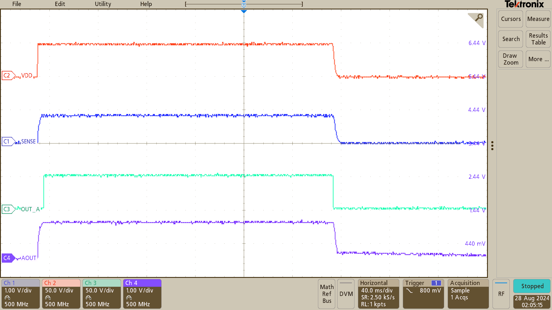
Figure 8-2
TPS37100 waveform