JAJSGL5C December   2018  – August 2019 TPS3840

PRODUCTION DATA.  

  1. 特長
  2. アプリケーション
  3. 概要
    1.     Device Images
      1.      代表的なアプリケーション回路
      2.      TPS3840 の標準的な消費電流
  4. 改訂履歴
  5. 概要 (続き)
  6. Device Comparison Table
  7. Pin Configuration and Functions
    1.     Pin Functions
  8. Specifications
    1. 8.1 Absolute Maximum Ratings
    2. 8.2 ESD Ratings
    3. 8.3 Recommended Operating Conditions
    4. 8.4 Thermal Information
    5. 8.5 Electrical Characteristics
    6. 8.6 Timing Requirements
    7. 8.7 Typical Characteristics
  9. Detailed Description
    1. 9.1 Overview
    2. 9.2 Functional Block Diagram
    3. 9.3 Feature Description
      1. 9.3.1 Input Voltage (VDD)
        1. 9.3.1.1 VDD Hysteresis
        2. 9.3.1.2 VDD Transient Immunity
      2. 9.3.2 User-Programmable Reset Time Delay
      3. 9.3.3 Manual Reset (MR) Input
      4. 9.3.4 Output Logic
        1. 9.3.4.1 RESET Output, Active-Low
        2. 9.3.4.2 RESET Output, Active-High
    4. 9.4 Device Functional Modes
      1. 9.4.1 Normal Operation (VDD > VDD(min))
      2. 9.4.2 VDD Between VPOR and VDD(min)
      3. 9.4.3 Below Power-On-Reset (VDD < VPOR)
  10. 10Application and Implementation
    1. 10.1 Application Information
    2. 10.2 Typical Application
      1. 10.2.1 Design 1: Dual Rail Monitoring with Power-Up Sequencing
        1. 10.2.1.1 Design Requirements
        2. 10.2.1.2 Detailed Design Procedure
        3. 10.2.1.3 Application Curves
      2. 10.2.2 Design 2: Battery Voltage and Temperature Monitor
        1. 10.2.2.1 Design Requirements
        2. 10.2.2.2 Detailed Design Procedure
      3. 10.2.3 Design 3: Fast Start Undervoltage Supervisor with Level-shifted Input
        1. 10.2.3.1 Design Requirements
        2. 10.2.3.2 Detailed Design Procedure
      4. 10.2.4 Design 4: Voltage Monitor with Back-up Battery Switchover
        1. 10.2.4.1 Design Requirements
        2. 10.2.4.2 Detailed Design Procedure
      5. 10.2.5 Application Curve: TPS3840EVM
  11. 11Power Supply Recommendations
  12. 12Layout
    1. 12.1 Layout Guidelines
    2. 12.2 Layout Example
  13. 13デバイスおよびドキュメントのサポート
    1. 13.1 デバイスの項目表記
    2. 13.2 コミュニティ・リソース
    3. 13.3 商標
    4. 13.4 静電気放電に関する注意事項
    5. 13.5 Glossary
  14. 14メカニカル、パッケージ、および注文情報

パッケージ・オプション

メカニカル・データ(パッケージ|ピン)
サーマルパッド・メカニカル・データ
発注情報

Design 2: Battery Voltage and Temperature Monitor

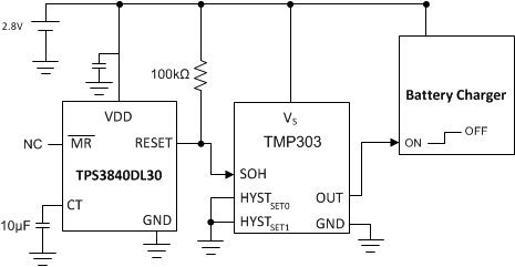
A typical application for the TPS3840 is battery voltage and temperature monitoring. The TPS3840 is offered in active-low or active-high output topologies and can operate above or below the voltage threshold meaning the device can be used as an undervoltage monitor as shown in Figure 49 or overvoltage monitor as shown in Figure 50. The TPS3840 can be used to monitor any rail above 1.6 V. In this design application, one TPS3840DL30 monitors the 3.3-V battery voltage rail and triggers an active-low reset fault condition if the battery voltage falls below the 3-V threshold. For overvoltage monitoring, another TPS3840DL30 monitors a 2.8-V battery and triggers a logic high at the 3-V threshold plus 100 mV hysteresis so at 3.1 V. Both applications monitor the battery temperature using TMP303, a push-pull, active-high temperature switch. A temperature fault is triggered if the battery temperature falls outside of a defined window temperature range set by the TMP303 variant chosen.
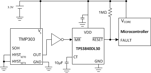
TPS3840 Typical_Application_2rev5.gifFigure 49. Low Battery Voltage and Window Temperature Monitoring Solution
TPS3840 Typical_Application_2rev6.gifFigure 50. Overvoltage and Window Temperature Monitoring Solution